
GaAs FET preamp

To construct the GaAs FET preamplifier, the following considerations should be taken into account:
1. **Component Selection**: The choice of a GaAs FET from the MGF family is crucial for achieving the desired performance characteristics. The MGF-1402 is particularly noted for its favorable noise figure and gain attributes.
2. **PCB Design**: The dead bug style assembly on a PCB is essential for minimizing parasitic capacitance and inductance, which can adversely affect high-frequency performance. The ground plane should be as continuous as possible to provide a low-impedance return path for signals.
3. **Transistor Mounting**: The use of a copper or brass shim for mounting the FET not only provides mechanical support but also aids in thermal management. The bending intervals must be precise to ensure that the components are securely held in place.
4. **Capacitor Selection**: Utilizing leadless disc or chip capacitors is recommended for their low inductance properties, which are beneficial in high-frequency applications. The placement of these capacitors should be as close as possible to the FET to minimize the length of connections.
5. **Shielding and Separation**: Maintaining separation between the RF and power supply sections is vital for reducing interference. A shielded enclosure will help to protect the sensitive RF components from external noise and interference, enhancing overall performance.
6. **Testing and Calibration**: After assembly, the preamp should undergo rigorous testing using calibrated equipment, such as the HP 8970 A and 346A, to verify noise figure and gain performance. Adjustments may be necessary based on test results to achieve optimal performance.
7. **Connector Quality**: The choice of connectors can significantly impact the stability and performance of the preamp. High-quality connectors should be used to ensure reliable connections and minimize signal loss.
By adhering to these guidelines, the GaAs FET preamplifier can be constructed to achieve excellent performance in terms of gain and noise figure, making it suitable for various RF applications.To build a GaAs FET preamp that has good gain and extremely low noise from readily available components. This preamp is stable with differing source and load situations. The circuit is built dead bug style on a piece of printed circuit board for a good ground plane. The FET sits on a stand made from a piece of copper or brass shim stock or strap " x 1- " bent into shape. This stand is used to support the source capacitors and the FET. Leadless disc`s or chip capacitors are used for the source capacitors, and output capacitor. Use generally accepted practices for vhf and uhf work. The power and RF section of the preamp must be kept separated. The use of a shield (screen) or separate compartment for the PS is suggested. The power supply section can be built on the under side of the preamp if double sided pc board is used, however this practice is not recommended if board is placed on the lid of a "Bud Box" which is common construction of this style preamp. The transistor stand is bent at these intervals, ", 1/8", ½", 1/8" to produce a _-_ (a little tough to produce with text, but you get the idea) The parts that have values listed on the schematic do not change from band to band.
Q1 is a Mitsubishi GaAs Fet from the MGF 1200, 1300, or 1400 family. My favorite is the MGF-1402. The completed unit should be placed into a shielded enclosure, especially if it is going to be placed at a repeater site. Alternately, the circuit can be placed into the receiver cabinet itself. Noise Figure tests were made by professional equipment to determine NF. A HP 8970 A and 346A were used for the tests. When constructed properly the units will be less than. 5 dB with. 40 to. 45 being typical. Gain is about 24 dB on 2 meters somewhat less on 220 and 440. The circuit is extremely stable when good quality connectors are used. N type or quality teflon BNC connectors are recommended on the 440 model. 🔗 External reference
Related Circuits
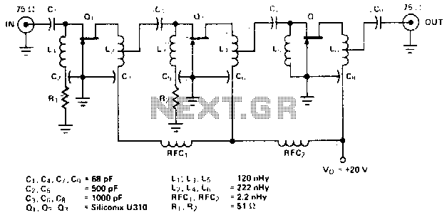
The amplifier circuit is designed for a center frequency of 225 MHz, with a bandwidth of 50 MHz at 1 dB, low input voltage standing wave ratio (VSWR) in a 75-ohm system, and a gain of 24 dB. Three...
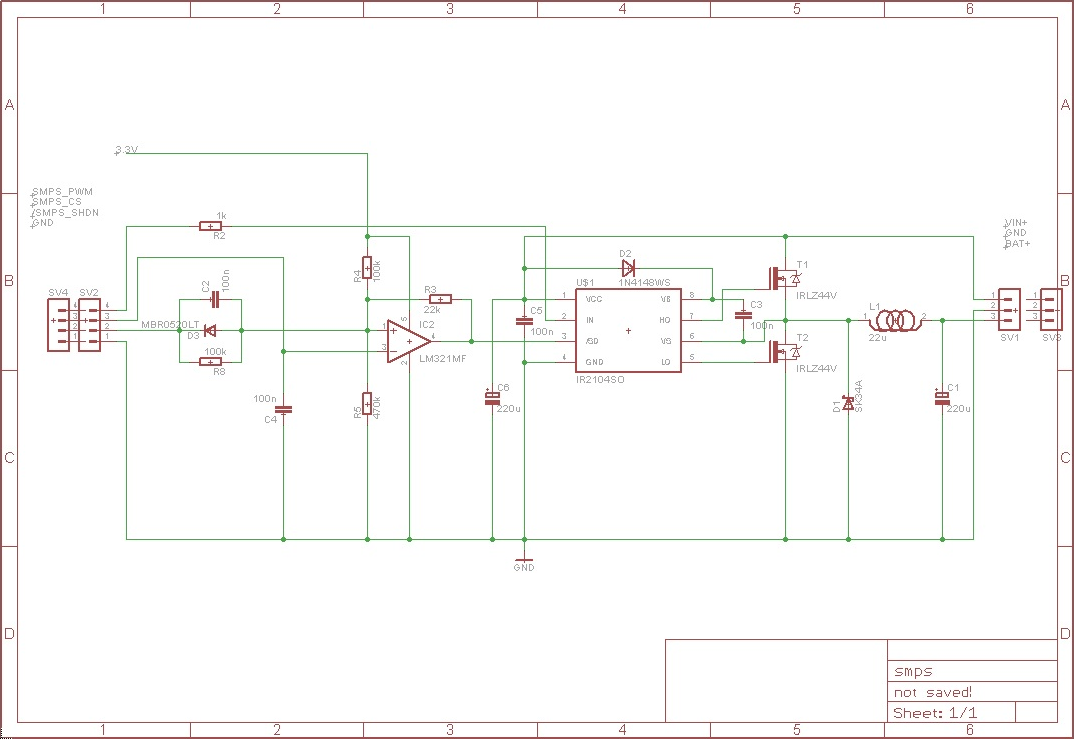
The circuit receives an input voltage (Vin), which is processed through a Switch Mode Power Supply (SMPS) utilizing two MOSFETs driven by an IR2104 driver. The output is directed to the battery positive terminal (Bat+). An LM321 operates as...
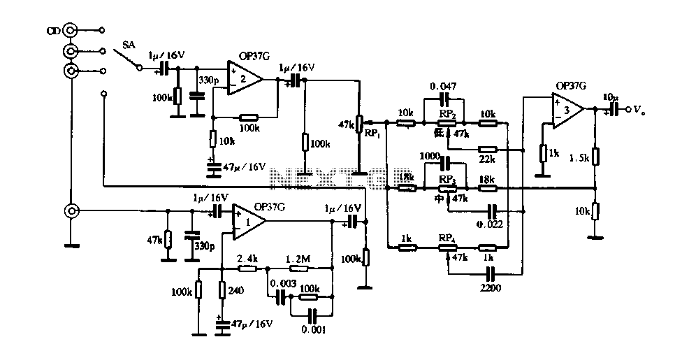
Figure 3 illustrates a circuit featuring the OP37, which is a multi-preamplifier configuration. The OP37 offers superior performance compared to the NE5534 integrated operational amplifier, as indicated in Table 3-3, which contrasts the parameters of both circuits. The table...

A decision has been made to construct a microphone preamplifier and tone control circuit that was featured on another website. The equalization section is identical to the one used in the... This microphone preamplifier and tone control circuit is designed...
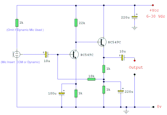
Both transistors should be low noise types. In the original circuit, BC650C was used, which is an ultra-low noise device. These transistors are now hard to find, but BC549C or BC109C are good replacements. The circuit is self-biasing and...
The project involves adapting a curve tracer schematic, likely based on Metzger's circuit from the early 1970s, to integrate an ADC capture system and output the data to a 320x256 ELD panel. Additionally, a serial output will be included...