
Gain buffer circuit

For achieving high speeds, discrete buffer components can be advantageous. Although their production is currently limited to 75 MHz, the employed GHz transistors provide a wide bandwidth, fast response, and minimal delay.
The circuit described utilizes a differential amplifier configuration, where the difference in amplified signals is critical for establishing biasing conditions for the transistors Q1 and Q2. Q1, functioning as a source follower, ensures that the gate-source voltage (VGS) is maintained at the appropriate level to match the input signal while providing a stable output. The 2000 pF capacitor connected to A1 plays a vital role in compensating for loop stability, preventing oscillations and ensuring reliable performance at high frequencies.
The inclusion of an RC network at the output serves to smooth out high-speed transitions, effectively reducing distortion and ensuring that the signal remains clean as it travels through the circuit. This network, in conjunction with the base-collector junction of Q2, enhances the circuit's ability to handle rapid changes in the input signal without introducing significant delay or distortion.
Feedback from the output of A2 back to the input around Q1 is crucial for improving the overall circuit performance. This feedback mechanism activates the bootstrapping effect, which enhances the input impedance and reduces the impact of load variations on the circuit's performance.
The choice of using Q1 and Q2 as a high-speed input buffer FET configuration is significant for applications requiring rapid signal processing. The open-loop nature of this configuration, while potentially prone to drift, is mitigated by the LTC1052, which stabilizes the circuit through its ability to compare filtered signals.
Furthermore, the mention of discrete buffer components highlights the potential for achieving even higher speeds in signal processing applications. The limitation to 75 MHz in production indicates a focus on optimizing the performance of these components, while the use of GHz-rated transistors suggests a design capable of handling a wide bandwidth with minimal signal degradation. This makes the circuit well-suited for high-frequency applications where speed and accuracy are paramount.The difference between these amplified signals is used to set the 's bias and hence Ql Q2 current channel. This Ql forces of V GS at all that is required voltage corresponding to the circuit input and potential output.
The capacitor of 2000 pF to Al provides stable loop compensation. The RC network at the output of Amnesty International that it obscures the edges at high speed coupled through Q2 's base-collector junction. A2 exit from the east also returned to the screen around Ql cause the door, the boot capacity of the circuit comes into force unless I pF.
Ql and Q2 constitute a simple, high-speed input buffer FET. Ql functions as a source follower, with the load current source Q2 setting the drain-source channel current. Normally, this open loop configuration would be quite drifty because there is no return current. The LTC1052 this function helps to stabilize the circuit by comparing the filtered output of a filtered version of the same input signal.
For very fast, the buffer component showed discrete alternative will be useful. Although its production is currently limited to 75 RNA, the transistors GHz employees provide a very wide bandwidth, fast and very little direction late.
Related Circuits
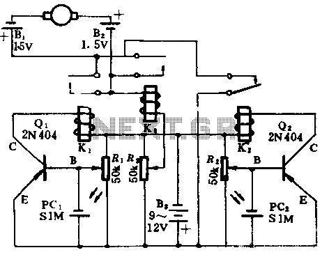
In the absence of light, photocells PC1 and PC2 exhibit high resistance, causing transistors Q1 and Q2 to remain off, which prevents the relay contacts K1 and K2 from closing. The battery B3 is connected through a potentiometer Rs,...
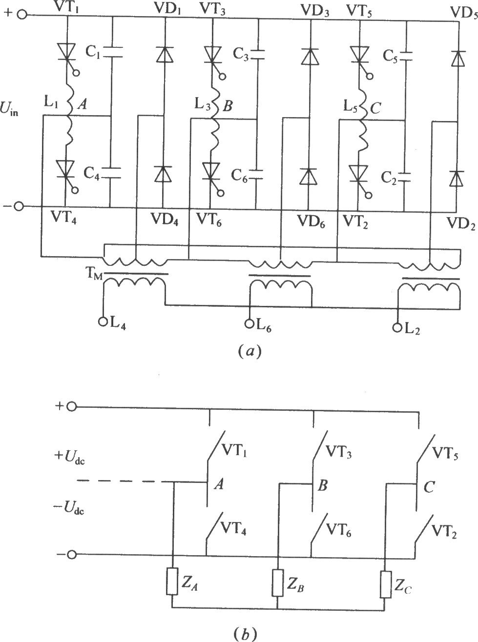
The figure illustrates a traditional three-phase bridge inverter circuit. Components VT1 to VT6 represent thyristors, while L1 to L6 are commutation reactors. Capacitors C1 to C6 serve as commutating capacitors, and the thyristor shut-off circuit is composed of two...
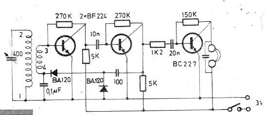
Oscillating circuits (coils) are constructed on a ferrite bar. For long wave reception, winding "1-2" consists of 135 turns, while winding "3-4" has 20 turns. For medium wave reception, winding "1-2" has 75 turns, and winding "3-4" has 7...
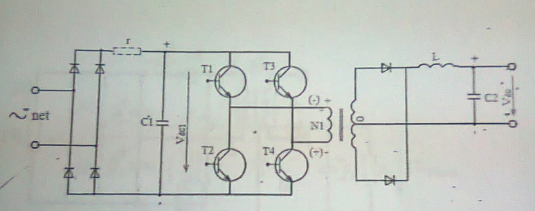
A power supply with frequent energy switching; however, the schematic is incomplete. An additional circuit is needed to control the voltage polarity converter, which consists of four transistors. This circuit generates high-frequency current pulses. Assistance is appreciated to explain...
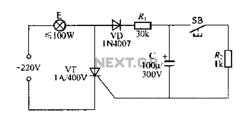
Figure 57 illustrates a simple delay lamp circuit that connects to lamp E using a two-wire connection. This design allows for the security bars to be installed directly, enabling replacement with a standard wall switch without altering the existing...
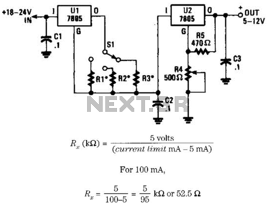
This voltage regulator and current limiter combination can be constructed using two 7805 regulators as illustrated. Resistors R1, R2, and R3 should be chosen to achieve a 5-V drop at the maximum allowable current limit. Switch S1 selects one...