
GMSK Demod

The GMSK_Demod circuit operates by leveraging the unique characteristics of Gaussian Minimum Shift Keying (GMSK), which minimizes the bandwidth while maintaining a low bit error rate. The coherent demodulation process involves a precise alignment of the reference carrier signal to the incoming modulated signal, which is critical for accurately recovering the transmitted data. The synchronization of the clock signal is equally important, as it directly influences the timing of the sampling process.
In practical applications, the performance of the GMSK_Demod can be affected by various factors, including signal-to-noise ratio (SNR), phase noise, and frequency offset. Therefore, implementing additional filtering and error correction techniques may enhance the reliability of the demodulation process. The use of sample-and-hold circuits ensures that the sampled values of I(t) and Q(t) remain stable during the decoding phase, allowing for accurate interpretation of the information sequence.
Overall, the GMSK_Demod component is a vital part of communication systems that utilize GMSK modulation, providing a balance between complexity and performance, making it suitable for various applications, including mobile communications and satellite systems.GMSK_Demod is a model of a suboptimal (an optimal receiver would require the Viterbi algorithm) coherent GMSK demodulator (refer to the GMSK_Recovery component). Noncoherent demodulation can be performed with the FM_Demod component. Pin 1 is the input for the GMSK modulated RF signal; pin 2 is the input for a reference RF carrier signal used to de
modulate the GMSK signal and obtain its inphase and quadrature components; pin 3 is the input for a clock baseband signal used to sample the demodulated inphase and quadrature signals. The reference RF carrier signal should be synchronized in frequency and phase to the modulated signal for proper demodulation.
The clock signal should have a duty cycle of 50 percent; its frequency should equal half the transmitted data rate; and, its phase should be adjusted so that the positive edge of the clock occurs at the instant when the eye of the demodulated inphase signal is maximum (therefore, the negative edge will occur when the eye of the demodulated quadrature signal is maximum). Coherent GMSK Demodulator Schematic shows the demodulator schematic. To understand the operation of this demodulator, note that GMSK is a digital phase modulation technique where the phase of the carrier G †(t), changes by G‚ ±G /2 radians (approximately) in a symbol period, depending on whether the input is G‚ ±1.
Let I(t) and Q(t) be the inphase and quadrature components of the GMSK signal. Let T S be the duration of an data symbol, and let 2 nT S, n=0, 1, 2, . be the instances when I(t) is sampled and (2 n+1)T S, n=0, 1, 2, . be the instances when Q(t) is sampled. The samples of I(t) and Q(t) then provide the following information about the phase of the modulated signal: By following the phase trajectory, the information sequence can be determined. In the demodulator circuit shown in Coherent GMSK Demodulator Schematic, the demodulated inphase and quadrature signals are sampled alternately and samples I (2 nT S ) and Q (2 n +1) T S ) are stored in the sample and hold components.
The logic gates then decode the information sequence X n, n = 0, 1, . from the samples based on The carrier and clock signal can be recovered from the modulated signal with the GMSK_Recovery component (see GMSK Demodulator with Carrier/Clock Recovery Component ). Or, ideal signals can be generated using N_Tones and Clock components, in which case the carrier and clock signals should be synchronized with the received modulated signal.
🔗 External reference
Related Circuits
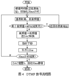
DTMF (Dual Tone Multi-Frequency) signaling is commonly used in telephone networks, including home phones, cellular phones, and SPC exchanges, for transmitting and receiving numbers. DTMF technology is also applicable in scenarios such as power line carrier communication. It is...
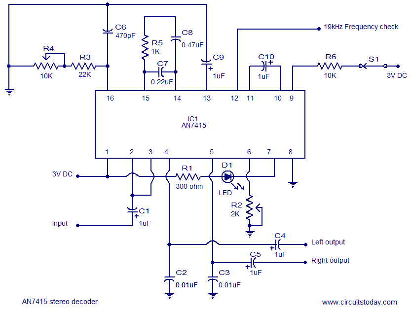
AN7415 based FM stereo demodulator circuit. 1.6 to 7V operating voltage range. High gain and low distortion. The AN7415 is a versatile integrated circuit designed for FM stereo demodulation applications. This circuit operates within a voltage range of 1.6 to...
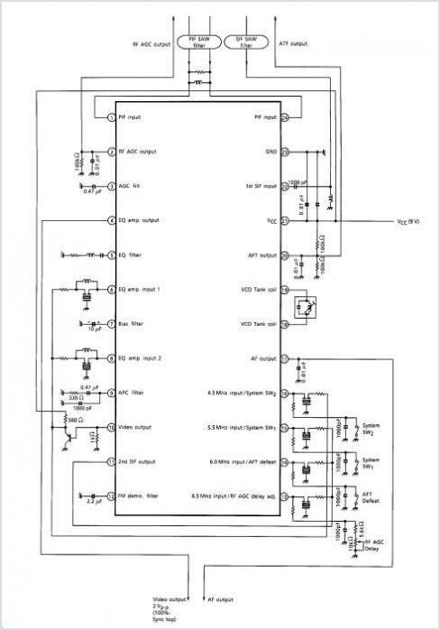
The TA1284FN is a TV tuner integrated circuit (IC) that combines a mixer and oscillator for VHF and CATV bands, a mixer and oscillator for the UHF band, and an intermediate frequency (IF) amplifier into a single chip. It...
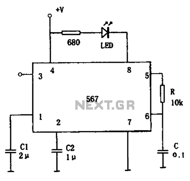
The FM demodulation circuit is illustrated in Figure 567. The FM signal is input at pin 3, and the demodulated signal is output from pin 5. The center frequency of the FM demodulation circuit is determined by the formula...
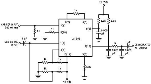
A simple single sideband (SSB) suppressed carrier demodulator circuit can be constructed using the LM1596 balanced modulator-demodulator integrated circuit (IC). The carrier signal should be applied to the carrier input port at an optimal level of 300 mVrms to...
The circuits utilize two FM Demodulator TDA2555 systems to execute the demodulation functions necessary in a dual sound carrier television system for demodulating the sound carriers. The distinction between the TDA2555 and TDA2557 lies in the number of stages...