
Headphone amplifier Class A circuit

The described circuit is a fundamental electronic design that effectively manages distortion and frequency response characteristics, making it suitable for various applications in audio and signal processing. The input resistance of 250K ohms indicates that the circuit is designed to interface with high-impedance sources, minimizing the loading effect on the preceding stage. This high input resistance is advantageous in applications where signal integrity is critical, such as in audio preamplifiers or sensor interfaces.
The output stage of the circuit is capable of driving loads from 100 ohms to 2K ohms. This range of load impedance suggests versatility in connecting to various downstream devices, including speakers, operational amplifiers, or other signal processing circuits. The ability to drive lower impedance loads (100 ohms) indicates that the circuit can handle higher current demands, which is essential in driving speakers or similar devices without significant distortion or loss of fidelity.
To ensure optimal performance, attention should be given to the design of the circuit's components, including the selection of resistors, capacitors, and any active devices such as transistors or operational amplifiers. Proper layout and grounding techniques will further enhance the circuit's ability to maintain low distortion and a wide frequency response, contributing to overall signal quality.
In summary, this circuit represents a well-thought-out design that balances simplicity with the necessary performance characteristics, making it suitable for various electronic applications where input impedance and load driving capabilities are critical.Even if simple the circuit, plirej` all condition, regarding the distortion and the response of frequency. The resistance of entry is 250K and the load that can drive is between 100R and 2K.. 🔗 External reference
Related Circuits
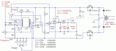
This is a simple function generator built around a single 8038 waveform generator IC. The circuit is capable of producing sine, square, or triangle waves within a frequency range of 20Hz to 200kHz. The function generator circuit utilizes the 8038...
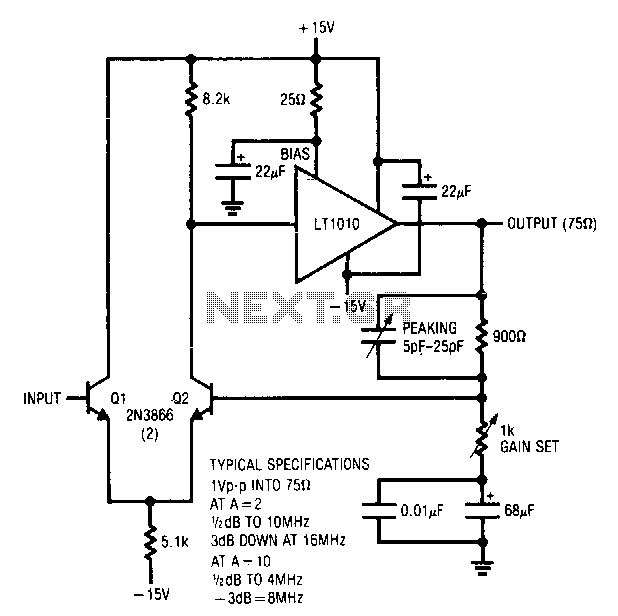
Q1 and Q2 create a differential stage that transitions into the LT1010. The capacitively terminated feedback divider provides a gain of 1, while permitting AC gains of up to 10. With a 20-ohm bias resistor, the circuit outputs 1...
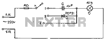
The figure illustrates a basic dimming lights circuit. The light intensity is controlled by a multi-speed control switch, designated as K. When switch K is set to position "1," the lights are turned off. In position "2," the light...
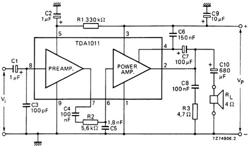
The following schematic illustrates the design of a 4 Watt Amplifier Circuit Diagram intended for portable radio applications, utilizing the TDA1011 integrated circuit from Philips Semiconductor. The 4 Watt Amplifier Circuit is designed to provide audio amplification in portable radio...
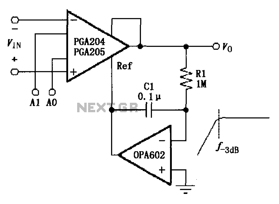
The circuit depicted in the figure features a programmable amplifier utilizing the PGA204/205 operational amplifiers in conjunction with the OPA602. The OPA602 op-amp is configured to establish a feedback reference point, while external components, specifically the capacitor C1 and...
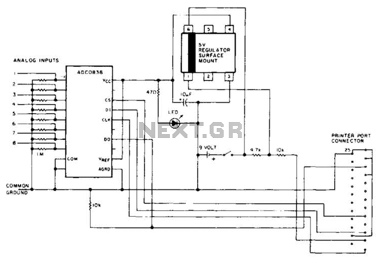
An A/D converter by National Semiconductor (ADC0838) converts 0 to 5 V analog inputs into a digital data format. A 9 V battery is utilized. The converter connects to the pointer port connector through a 25-pin connector. The ADC0838 is...