
Hi Pot tester schematic

The circuit design employs a center-tapped neon sign transformer capable of delivering high voltage outputs, which necessitates careful consideration of safety protocols. The transformer functions by converting low voltage AC input into high voltage AC output, which is then rectified to DC using appropriate rectification components. The rectification stage typically involves high-voltage diodes rated for the output voltage to ensure reliability and safety.
The inclusion of a variac allows for adjustable input voltage, providing control over the output voltage levels. The use of two 100W light bulbs in parallel serves as a current-limiting feature, which helps to protect the circuit from excessive current draw during operation. This is particularly important in high voltage applications where overcurrent can lead to component failure or create hazardous situations.
The voltage measurement setup, which includes a microamp meter and shunt resistor, is designed to provide accurate voltage readings at high potentials. Similarly, the current measurement circuit, utilizing a 100µA instrument with protective diodes, is crucial for monitoring the current flowing through the circuit without exposing the operator to dangerous voltages.
The design emphasizes insulation and creepage distance to mitigate risks associated with high voltage. The use of lexan and other insulating materials contributes to a safer operating environment. It is critical that all components are rated for the high voltage levels present in the circuit to prevent breakdown and ensure longevity.
In summary, this high voltage circuit design integrates several protective measures and features to ensure safe operation while providing high voltage outputs for testing purposes. Proper understanding and adherence to safety guidelines are essential for anyone attempting to replicate or work with this circuit.The design is based loosely on some ideas from K8CU and AG6K. However, I have simplified the circuit somewhat and used different components. The mechanical encapsulation is also different. I used LTspice to verify the tester before building it. The schematic is from the LTspice simulation (see below). I have also posted the simulation files so you can load them into your own LTspice simulator. The unit consists of a 700VA 12KV AC RMS output (nominal) center tapped neon sign transformer that I purchased on Ebay. The trafo was designed for less than 230V AC RMS nominal primary voltage. Therefore the transformer gives out a bit more than 12KV AC RMS when supplied from the 230V AC RMS mains in Norway.
After the rectifier I get approx 17-18 KV DC. The transformer is simulated by a sine voltage source in LTSpice. The transformer is insulated from ground in the tester for safety reasons. The schematic shows a gnd connection but that is only to get the Spice 3F4 solver to accept the netlist. It is recommended to insulate your tester from ground if you build one. There is a variac (not drawn on the schematic) in front of the transformer and the input is current limited by two 100W light bulbs in parallel (bulbs not drawn on the schematic).
The voltage metering circuit is a uA meter with a shunt resistor and the current measurement instrument is a std. 100uA instrument protected by back to back diodes (not drawn on the schematic). The instruments are at high potential so adequate protection must be implemented to prevent arcs to the operator.
The device under test (DUT) is drawn. Note that a working tube has much higher resistance than 100 megs that is the load in the simulation. However this is placed as a load test for the simulation to check smoothing of the output voltage. The chassis is built in plastic and lexan and I have ensured long creepage distances by utilisation of vertical lexan insulators.
There are no detected creepage currents at all even at full DC HV potential with my current design. WARNING: do not attempt to build this high voltage device unless you are experienced in electronics and high voltage circuits. Touching the HV leads may instantly kill you. I do not accept any responsibility for your use of this device. The schematic is not a complete circuit description. 🔗 External reference
Related Circuits

The circuit depicted in Figure 8 is a low-pass filter utilizing an eight-stage switched-capacitor configuration. The cutoff frequency of the circuit can be adjusted, with a clock frequency that can be modified to 1/100 of the original frequency. A...

The KCZ3 is an integrated three-pulse triggering component designed for use in three-phase half-bridge inverters. Each phase output pulse can reliably drive a high-power thyristor and is adaptable to various phase voltages. The electrical parameters are as follows: Phase...
The laser torch is an economical device with impressive cost-performance characteristics. Its primary feature is the exceptional performance of the condenser, allowing for an optical range of 1200 to 1500 meters. The beam remains focused and small even at...
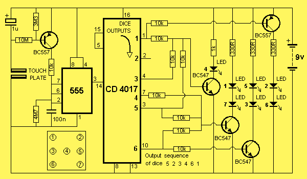
This project has two advantages over previous dice circuits. It produces a realistic readout as well as a slow-down feature. These combine to make it one of our most popular games projects. As can been seen in the photo,...
This application note provides valuable PC board layout, bypassing, and decoupling guidelines for customers who are implementing high-speed data converters in their designs. High-speed data converters are critical components in modern electronic systems, requiring careful consideration of their integration into...

This electric fencing solution is essential for operation in regions with dry ground. It includes a schematic for an Electric Fence Charger, originally created by KC Mylrea in 1972. The purpose of this system is to power electric fences...