
High-performance power supply LM334

The switching power supply circuit described is characterized by its ability to efficiently convert input voltage to a stable output voltage while minimizing power loss. The integration of the linear regulated power supply allows for enhanced performance in applications requiring precise voltage regulation. The circuit's high efficiency is particularly advantageous in battery-powered devices, where energy conservation is critical.
The voltage sampling circuit, comprising resistors R8 and R9, plays a crucial role in monitoring the output voltage. By providing feedback to the error amplifier, this arrangement ensures that any fluctuations in output voltage are promptly addressed. The error amplifier, formed by IC2 and VT2, amplifies the difference between the reference voltage and the sampled output voltage, adjusting the control signal to maintain a consistent output.
Moreover, the current limiting feature is essential for protecting the circuit from overload conditions. The adjustable reference voltage generated by IC1-a allows for flexibility in setting the maximum allowable output current. This is particularly useful in applications where varying load conditions may lead to excessive current draw. The output current is sampled through resistor R2, and the resulting voltage is compared to the reference voltage to produce an error voltage. This error voltage is utilized to modulate the operation of regulator VT1, ensuring that the output current remains within safe limits.
Overall, the described circuit is well-suited for applications requiring reliable power delivery with stringent voltage and current specifications. Its design effectively balances performance with safety, making it a valuable component in modern electronic systems. As shown in Figure as a switching power supply to work with linear regulated power supply. Its characteristics are: high efficiency, low dropout; having the ability to filter o ut high frequency ripple voltage and instantaneous voltage of the mutation; best suited to the needs of small loads; having a current limiting function. Figure by VD3, IC1-b and other components to generate the reference voltage. R8, R9 constitute a voltage sampling circuit for sampling the output voltage of the power supply. IC2 and VT2 and other elements constituting the error amplifier and shunt voltage regulator circuit. By comparing the reference voltage and IC2 amplify the sampled voltage, the driving regulator VT2, thereby stabilizing the output voltage.
By the VD1, IC3, VD2, IC1-a, VT1 and other elements constituting a current limiting circuit. VD1, IC3 and RP1 formed adjustable current limiting reference voltage generated by IC1-a reference to this voltage R2 (output current sampling resistor) comparing the sampled voltage amplification to form the error voltage. With the error voltage control the regulator VT1 working conditions, so as to stabilize and limit the output current.
Related Circuits
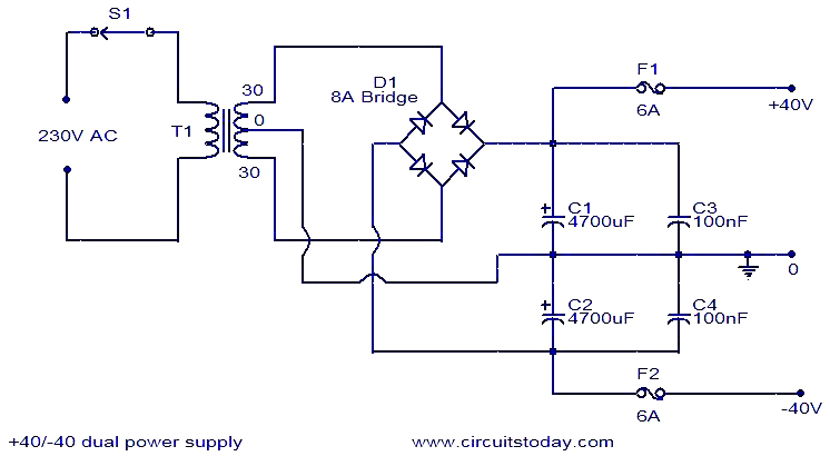
This 40V dual power supply circuit was designed to power a 150 Watt amplifier circuit. The transformer T1 steps down the mains voltage, while bridge D1 performs rectification. Capacitors C1 and C2 act as filters, and C3 and C4...
The following circuit illustrates a 2000W Power Amplifier Circuit Diagram. This circuit utilizes the BC560C transistor. Features include a robust design. The 2000W power amplifier circuit is designed to deliver high output power suitable for various applications, including audio amplification...
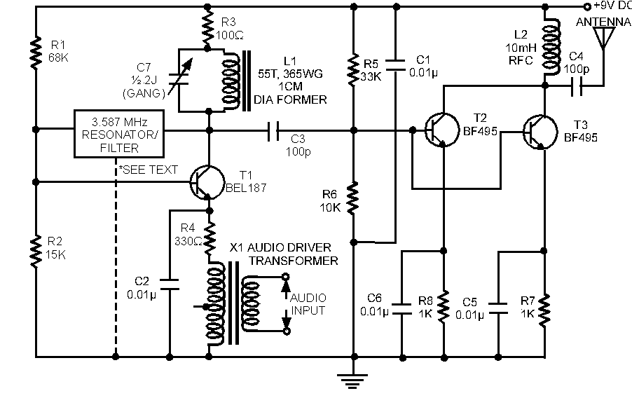
The circuit for a powerful AM transmitter using ceramic resonator/filter of 3.587 MHz is presented here. Resonators/filters of other frequencies such as 5.5 MHz, 7 MHz and 10.7 MHz may also be used. Use of different frequency filters/resonators will...
A novel supply voltage monitor which uses a LED to show the status of a power supply. This simple and slightly odd circuit can clearly show the level of the supply voltage (in a larger device): as long as...
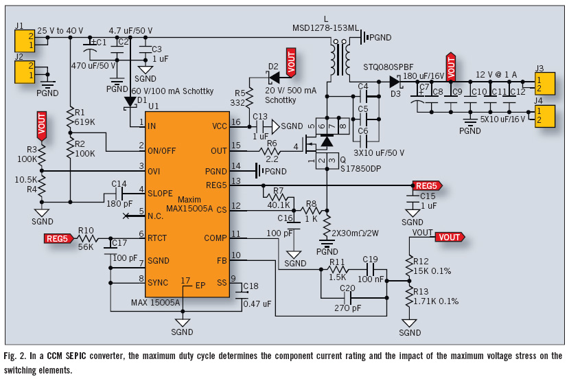
The Single-Ended Primary Inductance Converter (SEPIC) topology is an effective solution for automotive power systems that necessitate an output voltage that falls between the low and high values of the input voltage. The SEPIC topology is suitable for this...
The main component is the LG26 one-inch screens integrated with the FSP107-2PS01 two-in-one electrical power package, which utilizes a direct drive CCFL modulator tube. This setup is compatible with screens from other manufacturers, such as Samsung and AU, but...