
High Speed A/D converter 12-bit

To achieve this, the converter's zero point should be calibrated using an input voltage of 1.22 mV, adjusting R_trim until the LSB begins to appear (with all other bits remaining "0"). For full-scale calibration, an input voltage of 9.9963 V should be applied (10-V LSB), and R2 should be adjusted until the LSB starts to appear (with all other bits remaining "1"). In the bipolar mode, the signal range is from -5.0 V to 4.9976 V. The bipolar offset calibration is performed by applying a -4.9988 V input signal and adjusting R3 for LSB transition (with all other bits remaining "0"). Full-scale calibration in bipolar mode is determined by applying a 4.9963 V input signal and adjusting R2 until the transition to LSB occurs (with all other bits remaining "1").
This 12-bit converter is designed to facilitate precise analog-to-digital conversion in various applications. The unipolar mode allows for a wide range of input voltages, making it suitable for applications requiring high-resolution measurements within the specified range. The calibration process is crucial for maintaining accuracy and reliability in the output codes, ensuring that the digital representation of the analog signal is as close to the actual input voltage as possible.
In bipolar mode, the ability to handle negative voltages expands the versatility of the converter, allowing it to be used in applications that involve fluctuating signals around a zero voltage reference. The meticulous trimming process for both unipolar and bipolar modes ensures that the converter can achieve optimal performance, reducing errors caused by offset and gain drift over temperature variations.
Overall, the design of this 12-bit converter emphasizes precision and adaptability, making it a valuable component in various electronic systems that require accurate analog-to-digital conversion.This system performs a complete conversion of 12 bits in 10 p unipolar or bipolar. This converter is accurate to ± 12-bit LSB Y2 and a typical gain TC of 10 ppm / ° C. In unipolar mode, the system range is 0 V to 9.9976 V, with each bit having a value of 2.44 mY. For the accuracy of true conversion, an A / D converter must be trimmed so that, given the results just the exit code of input levels of Y2 Y2 LSB LSB below to above the exact voltage represents the code. Therefore, the converter zero point should be cut with an input voltage of 1.22 mY; R trim until the LSB is just beginning to appear in the exit (all other bits "0") . For the entire scale, use an input voltage of 9.9963 V (10-VI LSB LSB Y2), then cut R2 until the LSB is just beginning to appear (all other bits "1 ").
Bipolar signal range - 5.0 V to 4.9976 V. Bipolar offset cutting is done by applying a - 4.9988 V input signal and trimming R3 for LSB transition (all other bits "0"). On a large scale is determined by applying cutting R2 4.9963 V and the transition to LSB (all other bits "1").
Related Circuits
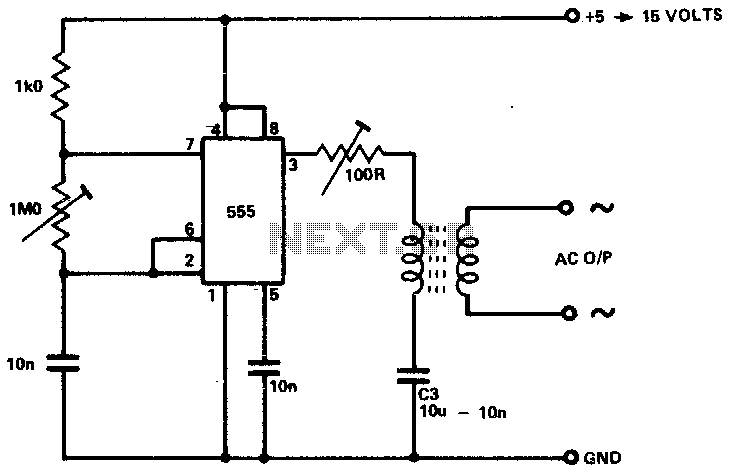
The circuit is designed to supply power for portable Geiger counters, dosimeter chargers, high resistance meters, and similar devices. The 555 timer integrated circuit (IC) operates in its multivibrator mode, with the frequency adjusted to optimize the characteristics of...

The TPS6420x controller is designed to operate from one to three series-connected cells or from a 3.3 V or 5 V supply obtained from a USB port. At its output, it can produce 3.3 V at 2 A, suitable...

This circuit is designed for higher input or output voltages in an L200 voltage regulator. It addresses issues that arise when input or output voltages exceed the regulator's specifications. The circuit incorporates external components, including a transistor that absorbs...
The objective is to enhance information transmission by utilizing articles. Please contact us via email at [email protected] within 15 days if there are any issues related to article content, copyright, or other concerns. The articles will be removed promptly. To...
High Current Variable Power Supply Circuit Diagram. The widely used variable voltage regulator IC LM317 can handle a maximum current of only 1 ampere, making it unsuitable for applications requiring a high current variable power supply. The design of a...

The operation of the converter is based on the weighted addition and transfer of the analog input levels to the digital output levels. It consists of... The converter functions by utilizing a weighted summation technique to process analog signals and...