
Higher Input Or Output for L200 Voltage Regulator

This L200 voltage regulator circuit is effectively designed to manage high input and output voltages, ensuring reliable performance while preventing damage to the components. The transistor's role in absorbing excess voltage is crucial, particularly in scenarios where input voltages may exceed the regulator's limits. The consideration of the safe operating area (SOA) for the BDX53 transistor is vital, as it ensures that the device operates within its safe limits, thereby enhancing the circuit's longevity and reliability.
The digital voltage selection feature allows for flexible output voltage control, making the circuit adaptable to various applications. The voltage divider formed by the resistors enables precise voltage adjustments, while the emitter follower configuration provides the necessary buffering to maintain stable operation. This configuration is particularly beneficial in applications where the load may vary, as it permits the zener diode to maintain a consistent reference voltage.
The inclusion of a dropping resistor in the zener regulator design is fundamental for achieving the desired output voltage. By calculating the resistance value based on the supply voltage and desired output current, the circuit can maintain efficiency and stability. The low-dropout regulator design is especially advantageous in applications requiring minimal voltage loss, allowing for effective regulation even at low load currents.
The high-power LED driver circuit demonstrates the versatility of the L200 regulator, showcasing its capability to drive LEDs efficiently. By utilizing a buck/boost converter controller, the circuit can adapt to varying input voltages and maintain a consistent output current to the LED, making it suitable for applications ranging from general lighting to specialized illumination tasks. This design approach not only enhances the efficiency of LED usage but also contributes to overall energy savings, making it a practical solution for modern lighting needs.This is higher input or output for L200 voltage regulator circuit. This circuit is designed to solve the problem that occurs when the input or output voltages are higher than the device can produce. This circuit uses the external components. Here is the circuit : The transistor is used to absorb the excess voltage when there are high input voltage
. The SOA of the preregulation transistor and the dissipated power should be calculated. The maximum input volage that can be reached if we use BDX53 is 56 V, so the Vce on transistor is 20V with load current o 2A the operation point remains inside SOA. The ripple at the input of the circuit is reduced by preregulation, so it can recieve an output voltage with negligible ripple.
When we need a high output voltage, we can use a second zener, Vz, that is used to refer an IC`s ground pin to a potential other than zero. To protect the output from short circuit, this circuit uses diode D1. [Source: STMicroelectronics Application Note] This is digital voltage selection control circuit. This circuit uses L200 Regulator. It can be used to regulated the output voltage digitally. Here is the circuit : A combination of P2, R3, R2, and R1 with R5 form voltage divider Continue reading †’.
Buffering for the zener is provided by the impedance matching and current amplifying characteristics of the emitter follower and draw less current from it. To a Zener regulator, it`s a useful adjunct. The capacitor on the right circuit is used Continue reading †’. The figure below show us a zener regulator. The essential component is the dropping resistor R which the value given by (V-Vo)/I, where I is the desired output plus 10%.
As long as the supply voltage V is constant, the Continue reading †’. This is a Low-dropout (LDO) Regulator circuit, constructed by using only a single PNP transistor. This circuit is directly related to load current. At very low values of load current as little as 50 mV. This circuit has maximum specified Continue reading †’. This is a wide input-voltage range high-power LED driver circuit. This circuit based on a buck/boost converter controller regulates current to a white LED. This circuit can be used to replace incandescent bulbs, it efficiently match the LEDs to available Continue reading †’. 🔗 External reference
Related Circuits
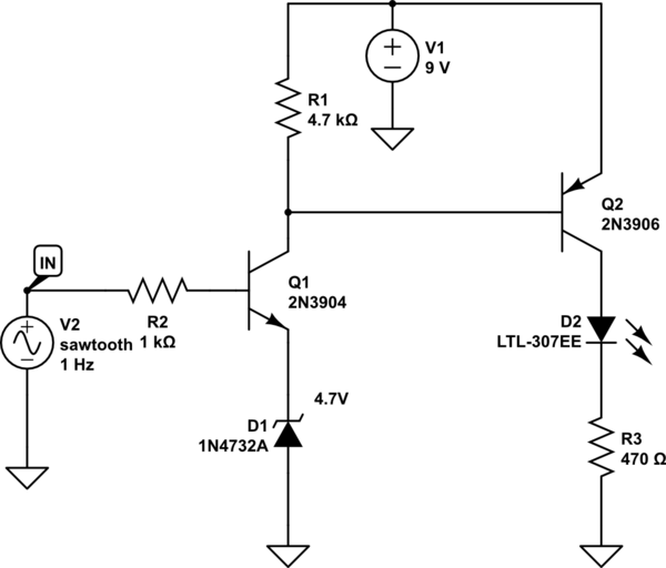
A LED is used to indicate when a DC voltage reaches 5 volts or more. The LED should be fully illuminated at 5 volts and not dim at 4.5 volts or lower. The circuit should be constructed using discrete...
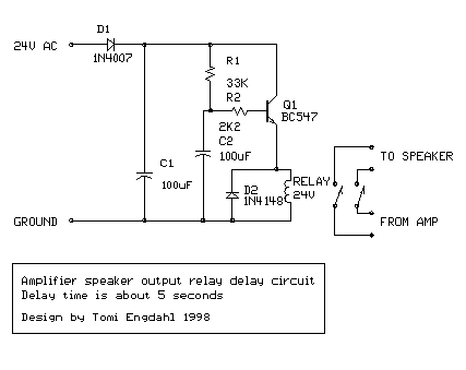
This is a simple circuit designed for an audio amplifier project to control the speaker output relay. The purpose of this circuit is to manage the relay that activates the speaker output in the audio amplifier. The circuit is...
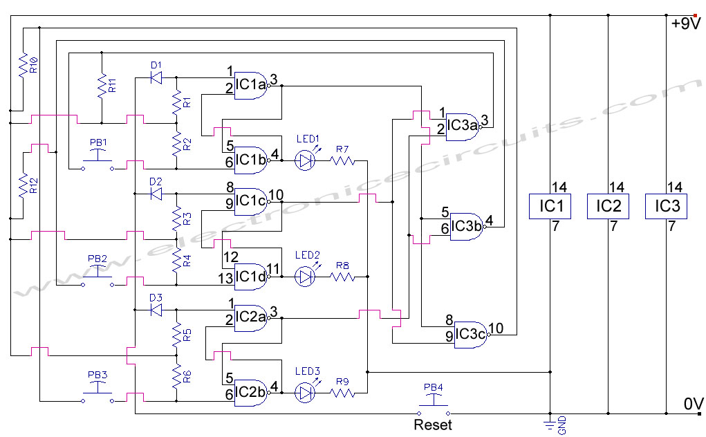
First Response Monitor, Input Selector, Game Circuit. This circuit is utilized for first response applications as it aids in monitoring various responses in games. The First Response Monitor circuit is designed to facilitate real-time monitoring and selection of input signals...
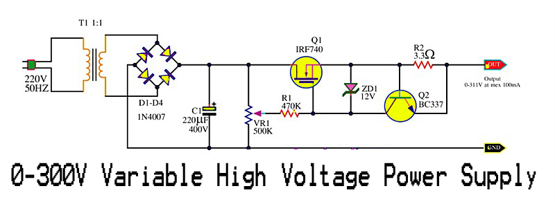
This is a variable high voltage DC power supply circuit that allows for customization of the output voltage ranging from 0 to 311V DC. It includes a current limit protection feature set at approximately 100 mA. The power MOSFET...
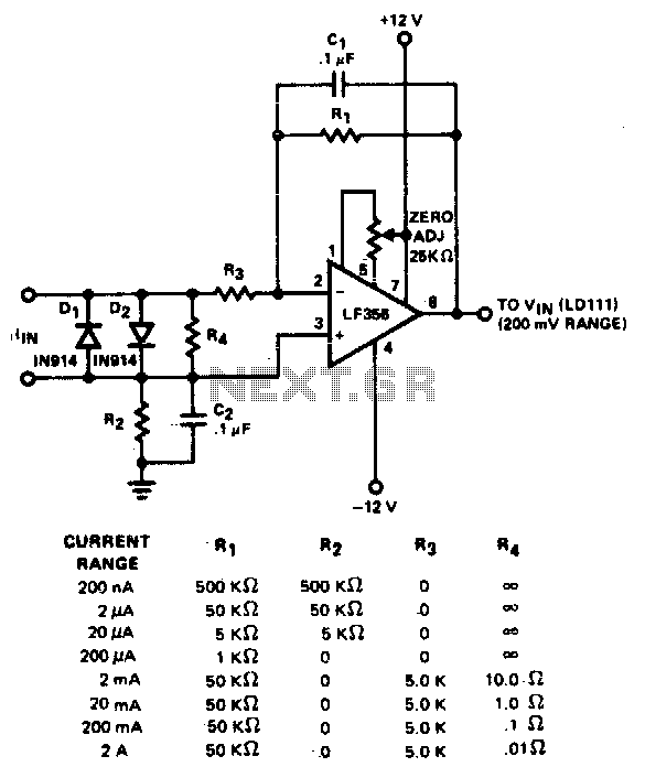
The converter features eight decades of current range. The circuit is intended to be used with the 200 mV range of a DVM. The described converter circuit is designed to accommodate a wide range of current measurements, spanning eight decades....
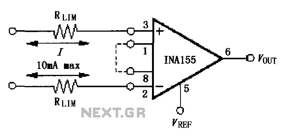
The input current protection circuit is illustrated in FIG, utilizing INA155/156. The INA155 features internal electrostatic discharge (ESD) protection diodes that become active when the input voltage exceeds the supply voltage by 500mV. In this scenario, the protection diodes...