
High Voltage Converter Circuit

The high voltage converter circuit utilizes a step-up transformer or a charge pump configuration to achieve the desired output voltage levels. The circuit's design typically includes a switching element, such as a MOSFET or IGBT, which rapidly alternates the input voltage to create a high-frequency signal. This signal is then fed into a transformer or capacitor bank that boosts the voltage to the specified levels.
In version 1, the output voltage is regulated to a maximum of 3 kV. This may be accomplished through feedback mechanisms that monitor the output voltage and adjust the switching frequency or duty cycle of the switching element to maintain a stable output. Version 2 extends this capability, allowing for an output voltage of up to 10 kV, which may require additional components such as high-voltage diodes and capacitors designed to handle the increased voltage levels.
Safety precautions are critical in the design of such high voltage circuits. Proper insulation, grounding, and protective components must be implemented to prevent electrical hazards. Additionally, the circuit may include features such as over-voltage protection, current limiting, and thermal management to ensure reliable operation.
The power supply's input stage must be designed to handle the initial 30 volts efficiently, while the output stage must be capable of managing the high voltage safely. The choice of materials and components is essential to ensure the circuit's longevity and performance under high voltage conditions.
Overall, this high voltage converter circuit serves applications that require high voltage outputs, such as in scientific experiments, industrial equipment, or specialized electronic devices.Starting from a 30 volt power supply this high voltage converter circuit can deliver a voltage between 0 to 3 kV (version 1) or from 0 to 10 kV (version 2). 🔗 External reference
Related Circuits
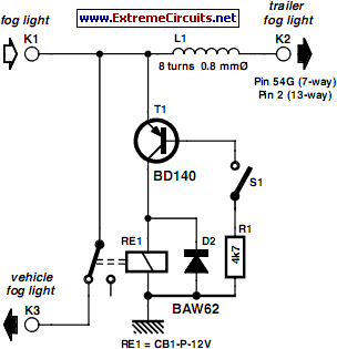
In many countries, it is now mandatory or at least recommended to have a rear fog light on a trailer, with the additional requirement that when the trailer is attached to the vehicle, the rear fog light of the...
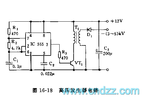
The high voltage generator depicted in figure 16-18 utilizes the 555 timer IC as its primary component. The oscillating voltage produced is enhanced through a step-up transformer. The astable multivibrator configuration comprises the 555 timer along with resistors R1...
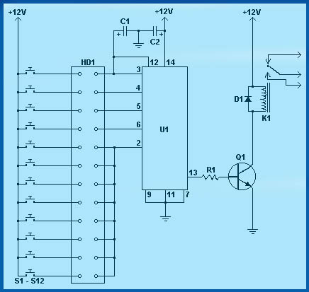
Circuit diagram schematics of electronic keys, electronic locks, digital electronic locks, transistor code locks, and combination electronic locks. The circuit schematics for electronic locking mechanisms encompass a variety of designs tailored to enhance security and convenience in access control systems....
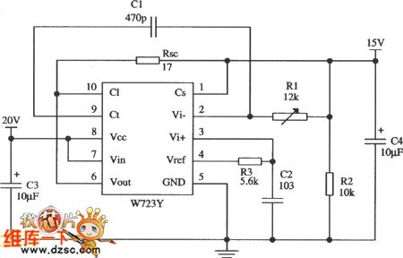
The application circuit depicted below features an output voltage that exceeds the referenced voltage. It utilizes the W723 multi-port adjustable positive voltage regulator, which incorporates current limiting protection. The output voltage can be adjusted within a range of 7V...
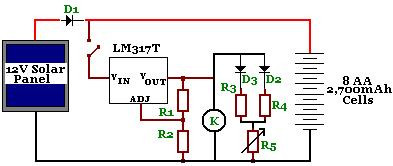
The circuit is designed to power a CCTV camera, provide lighting inside a nestbox, and charge batteries using a photovoltaic (PV) solar panel. It includes a circuit diagram for a solar-powered wireless CCTV camera with battery backup. D1 is...
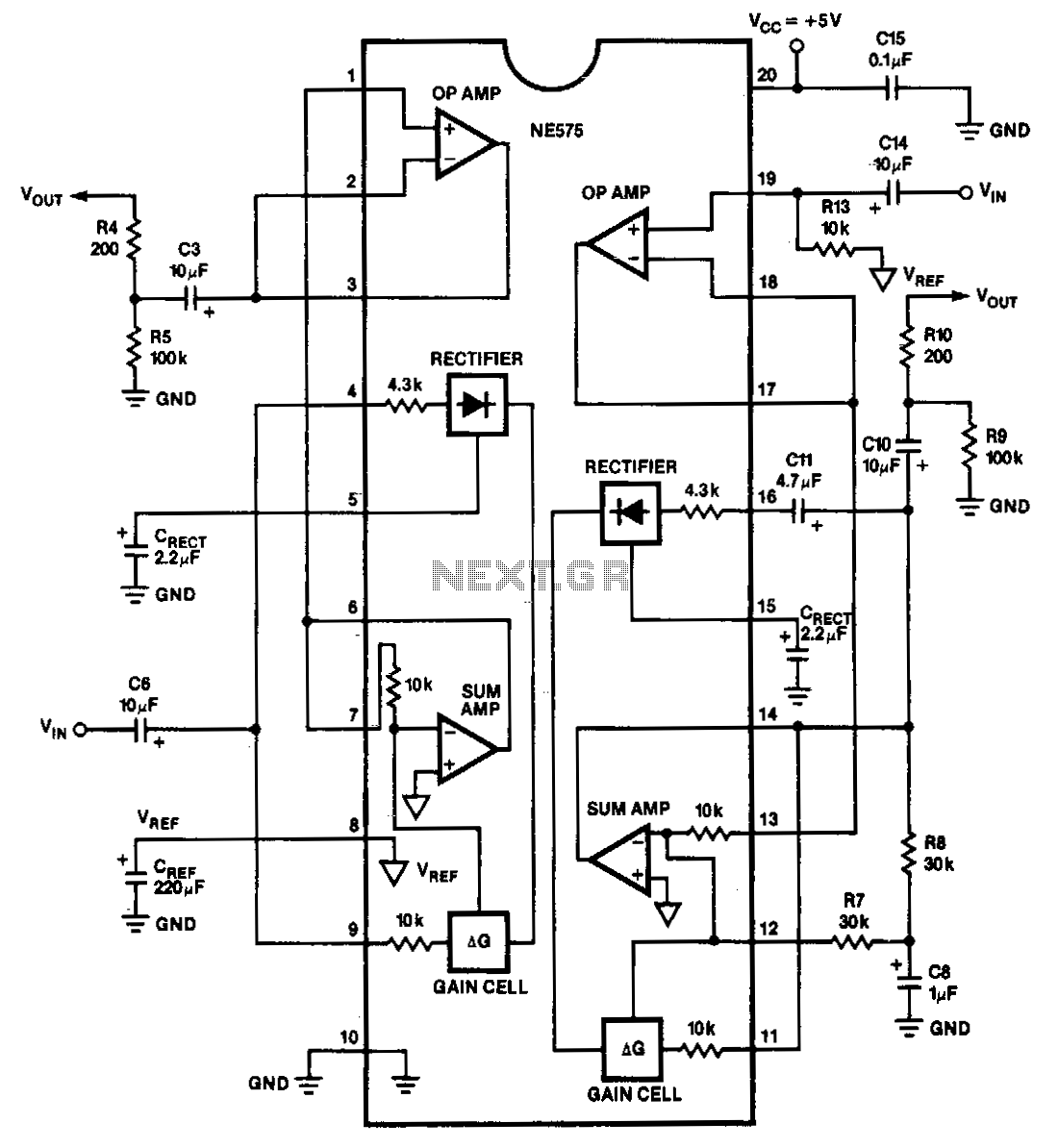
The NE575 is a dual-gain control circuit designed for low voltage applications. Channel 1 acts as an expander, while Channel 2 can be configured for expander, compressor, or automatic level controller (ALC) applications. The NE575 dual-gain control circuit is specifically...