
Homebuilt video digitiser MkII circuit description

The circuit design involves several key components that facilitate the digitization process. The core of the system relies on the ADC, which performs analog-to-digital conversion of the composite video signal. The high-speed 256kB field memory serves as a temporary storage solution, buffering the digitized data before it is transmitted to the PC. The video timing logic is crucial for synchronizing the data capture process, ensuring that the samples align with the video signal's timing characteristics.
In addition to the main components, the circuit also incorporates various passive components that help filter and stabilize the signals, ensuring high-quality digitization. The power supply circuitry is designed to provide stable voltage levels to the entire system, which is critical for reliable operation. The PCB layout should take into account the signal integrity by minimizing trace lengths and using appropriate grounding techniques to reduce noise and interference.
For users interested in adapting the design for different ADCs, it is recommended to carefully analyze the timing requirements and electrical characteristics of the chosen component to ensure compatibility with the existing architecture. This may involve adjusting the clocking scheme or modifying the interface logic to accommodate different data rates. Overall, this project presents a versatile solution for capturing and digitizing video signals, with potential for further enhancements and adaptations based on user needs.A "video-digitiser" (also known as a "frame grabber") captures still pictures frames from a TV set, video camera, or video recorder, etc. , and forwards them to a computer for display, storage, or general manipulation. This document describes the MarkII version of a home-built digitiser which interfaces to an EPP parallel port on IBM PCs.
MkII supports colo ur captures (PAL/NTSC decoding in software). Note: the Bt218 chip, around which this project is based, ceased to be manufactured during the year 2000. If you want to build this project as shown, ensure you can get some old stock! Alternatively, you could adapt the circuit to work with a different low-cost ADC, such as the TDA8703 from Philips.
I have not done this myself yet, so cannot offer details. Any PC hardware capable of running the operating systems mentioned should run the software adequately, though as always, a faster PC will often result in better performance. In particular, colourisation will be very slow on anything sub-Pentium! An EPP-type parallel port is required (though with software modifications, a simple bi-directional port would be useable, with poorer speed) Still only captures one of the two interlace fields (though often the second one would lead to motion blur anyway.
). Limited by mere 256kB of buffer. Published design captures odd/even field at random, though by simple modification you could ensure one or the other is guaranteed. Digitisation clock arrangement shown is not fully phase-locked to the linesync. A proper line-locked sampling clock could quite easily be implemented as an extension to the project.
In general, horizontal resolution is decreased in domestic video recording formats (and colour is really seriously degraded). Use off-air signals from a good aerial for best results! (This image is from only one field, so the height needs to be doubled to obtain the correct aspect ratio).
It was digitised with a 14. 161Msps clock, partially phase-locked to the line-sync. The ADC converts the incoming composite video signal to a digital representation, sampled typically at 15MHz. This data rate is far too fast for the parallel port to cope with directly, so instead the circuitry is arranged so that data from ADC is fed into a high-speed 256kB field memory.
Video timing logic uses line and field synchronisation signals from the sync-separator to ensure that storage begins and ends at field boundaries, and that a fixed number of samples (pixels) are collected for each video scan line. PC parallel port interface logic controls the output of data from the field memory to the host PC, and temporarily halts the refreshing of the image in the memory while data is being read out.
The MSM518221A-3Z is supplied in a "ZIG-ZAG" package, with two rows 0. 1" apart, of pins on 0. 1" spacing, with the two rows offset by 0. 05". This will not be an issue if designing a PCB, but for breadboard or Veroboard construction you will need to make an adapter! For convenience, the circuit is drawn in three sheets: 1) showing the analog and digital video signal path, including parallel port interface, 2) showing the clock and video timing, 3) the voltage regulator.
MSM518221 - WE enables data to be written and forward the Write pointer, IE when low, allows the write pointer to be forwarded, but inhibits overwriting of data. Reset Write Pointer (RSTW) is semi-synchronous - supposed to only lower for one cycle at a time - does NOT hold the Write Pointer at the start indefinitely!
This explains why some of the WE logic is less simple than it might be. CAUTION if modifying my design! On the Bt218KP the colour subcarrier trap is shown with component values for UK standard PAL: for NTSC, use two 220pF capacitors in paralllel to make 440pF to attenuate the 3. 5MHz signal. The subcarrier trap is ONLY required when obtaining black-and-white captures from colour signals, or when the sampling rate is too low to sample Fsc proper
🔗 External reference
Related Circuits
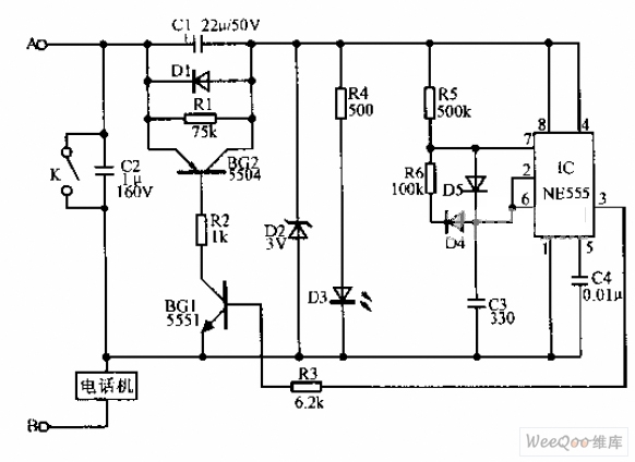
A simple telephone time lock circuit is depicted in the provided diagram. In this circuit, BG1 and BG2 function as electronic switches that are controlled by the IC NE555. When the telephone is on-hook, the DC resistance of the...
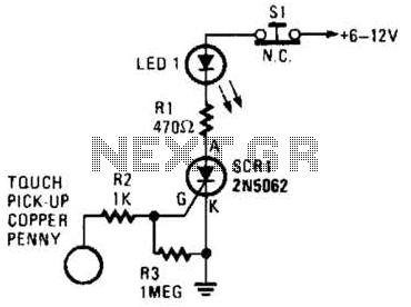
When the touch-on contacts are bridged, pin 6 of U1 goes low, which forces its output (the set output) at pin 4 to go high. That high divides along two paths; in one path, the output is applied to...
This caller ID circuit utilizes the Motorola MG145447 IC chip. The service must be available from your local phone company for this circuit to function properly. The caller ID circuit based on the Motorola MG145447 IC chip is designed to...
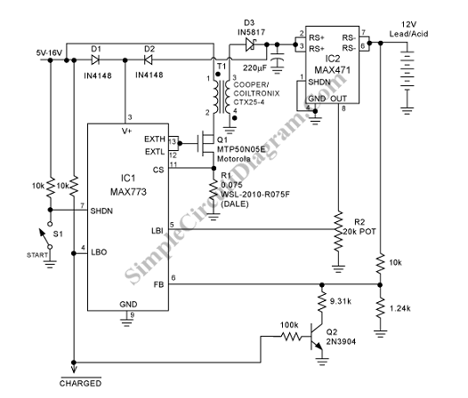
To charge lead-acid batteries, a circuit can be utilized that consists of a current-limited power supply and a flyback converter topology. The described circuit for charging lead-acid batteries employs a current-limited power supply in conjunction with a flyback converter...
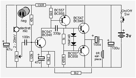
The following circuit presents a Mini Audio Amplifier Circuit Schematic Diagram. Features include a power consumption of less than 3mA, a small output, and the use of a push-pull configuration. The Mini Audio Amplifier Circuit is designed to amplify low-level...
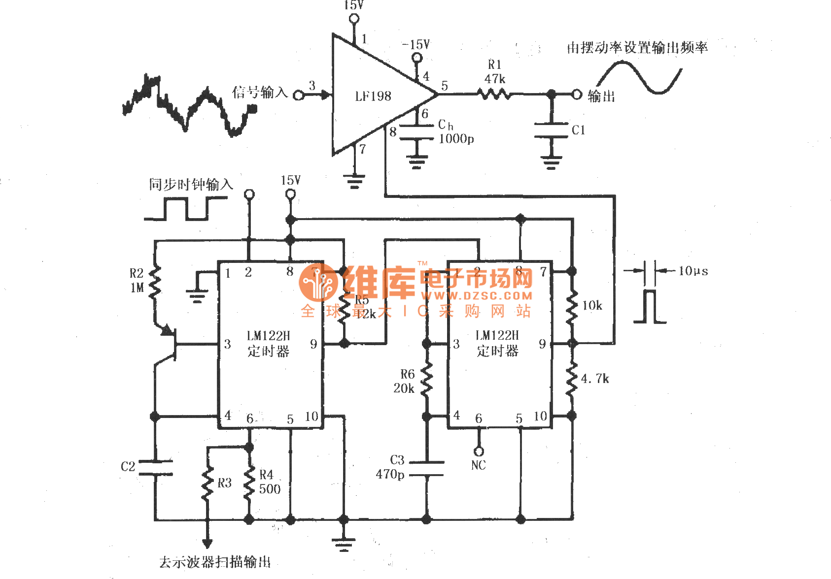
A synchronous clock signal is fed into a cascade of timer circuits composed of two LM122H devices. The synchronization clock is then converted into a pulse of the desired width, which is added to the LF198 logic end (pin...