
Homemade PC Boards

The circuit is designed to control a two-digit display representing minutes, utilizing two shift registers to manage the data output to the LEDs. Each of the 30 resistors serves to limit current to the corresponding LEDs, ensuring proper brightness and preventing damage. The shift registers facilitate the serial input and parallel output of data, allowing for efficient manipulation of the display digits. The schematic provides a clear representation of the interconnections between the components, illustrating how the shift registers interface with the LEDs and resistors.
The decision to create a custom PCB stems from the limitations of standard prototyping boards, which often do not allow for optimal component arrangement. The utilization of PCB design software simplifies the process of creating a layout that reflects the desired circuit functionality. The chosen software, ExpressPCB and ExpressSCH, not only allows for schematic drafting but also provides an integrated platform for PCB layout, ensuring that all connections are accurately represented.
Home PCB fabrication offers a practical solution for rapid prototyping, particularly for one-off designs. The method of using a laser printer to create an etch-resist mask is both accessible and cost-effective, allowing for the quick turnaround of prototypes. The challenge of aligning masks for a double-sided board requires careful planning and execution, with the potential for error if images are not correctly oriented prior to the transfer process.
Overall, this circuit design exemplifies the integration of digital logic with practical electronic components, demonstrating the ability to create a functional and visually informative display. The detailed approach to both the design and the prototyping process reflects a commitment to achieving a reliable and effective electronic solution.Control the two digits representing minutes; this circuit includes two shift registers, 30 resistors, and 30 LEDs. (All told, a particularly simplecircuit, really. ) Here`s the schematic: As I came closer to completing the circuit design, it occurred to me that trying to solder all of these components on a simple prototyping circuit board would be onerous at best.
(If you`ve ever done this kind of thing before, you know what I`m talking about!) Typically, prototyping boards have a matrix of pads for placing components, but no embedded traces connecting components to each other (or, if they have pre-printed traces, they are usually not in the most useful places). So I began researching designing a printed circuit board specifically for this circuit. There`s a plethora of freeware available to download for this purpose; many packages come with schematic drafting software as well, and are able to link the PCB design to the schematic, which greatly assists with ensuring traces connect the correct pads.
The package I chose was ExpressPCB and ExpressSCH; I like the interface and the company provides low-cost PCB board printing, if you`re willing to wait a little while for them. (For the record, I`m not endorsing their product or their company per se-it works for me, but it may not work for you.
) Then I got restless. I didn`t want to wait the month for ExpressPCB to print and ship my board. I wanted it right now! (I mean, the name of the company is "express, " after all. ) I remembered that a few months ago I had stumbled on a website with some crazy scheme for home-printing PC-boards, using some complex combination of laser printers, acids, and duct tape or something. So I did some additional researching and discovered that printing a PC-board at home is much simpler than I imagined, and significantly cheaper than having a professional shop do it, especially if I was only doing one-off boards.
There are dozens of sites which describe the method (here`s one ). Essentially, you create an etch-resist mask of the printed circuit design by printing it (using a laser printer) on glossy paper, then transferring the laser toner to a blank board using a hot iron. Once the mask is transferred, you drop the board into an acid solution (available at Radio Shack), which eats away any copper not covered by the laser-toner mask.
After some cleaning with acetone to remove the toner from the finished/etched board, you`ve got a shiny new printed circuit board! Of course, not one for doing anything easily, I had to go and design a two-sided board; this adds the complication of having to ensure that both masks are aligned when they are applied.
By lining up the masks face to face and taping them together along one side then sandwiching the board between them, I was able to solve this problem pretty easily. Or so I thought. Turns out, when I made my first board, I managed to flip one of the images in the wrong direction, so they no longer lined up properly.
(I checked all the edges, but never bothered to check the pads themselves, and didn`t discover the mistake until cleaning off the toner. ) 🔗 External reference
Related Circuits
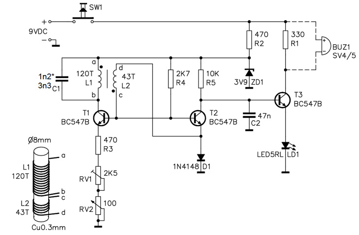
A simple home project can quickly become problematic if it encounters electric cables, gas, or water pipes, or the central heating system. Using a metal detector allows one to check for metal objects within walls, ceilings, or floors beforehand....
Instructions for constructing a 1kW synchronous rotary spark gap (SRSG) Tesla Coil. This device operates using mains power and is powered by a 1kVA (10mA, 10kV) neon sign transformer (NST). The construction of a 1kW synchronous rotary spark gap Tesla...
Instructions for constructing a simple Kirlian effect camera to capture high voltage corona discharges around objects, also referred to as aura photography. The Kirlian effect is a phenomenon where high voltage electrical discharges create a visual representation of the energy...
The circuit operates by sending ringing pulses through capacitor C1, resistor R1, and diode D2 to charge capacitor C2 to a voltage of 6V. This voltage causes transistors N1 and N2 to reverse, which activates V1, the analog hook,...
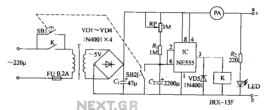
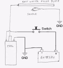
The homemade disinfectant circuit described in this example utilizes an electrolytic salt solution method to produce sodium hypochlorite (NaCl), which can be used for disinfecting living supplies for students. The circuit consists of a power circuit and a timing...
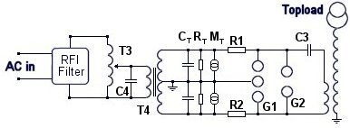
DIY Homemade Tesla Coil Tuner. Instructions for constructing a Tesla Coil Tuner using readily available components. Determine the resonant frequency of Tesla Coil components. A Tesla Coil Tuner is an essential tool for optimizing the performance of a Tesla coil...