
How to Make a Cell Phone RF Signal Detector Circuit

The circuit utilizes the LM324 IC, which contains four op-amps that can be configured for various applications. In this particular setup, the op-amps are arranged in a cascading configuration to maximize the amplification of RF signals. The use of a non-inverting configuration allows for a straightforward gain calculation, defined by the formula \( G = 1 + \frac{R_f}{R_{in}} \), where \( R_f \) is the feedback resistor and \( R_{in} \) is the input resistor. This design choice ensures that the circuit can amplify weak RF signals without inverting their phase, which is critical for accurate signal detection.
The antenna plays a pivotal role in capturing RF disturbances. It is recommended to use a simple wire antenna, which can be easily constructed by cutting a length of wire to an appropriate size based on the frequency range of interest. The antenna should be connected to the non-inverting input of the first op-amp, allowing it to receive RF signals from the surrounding environment.
For stability, it is essential to carefully select the feedback resistor values. While increasing resistance enhances sensitivity, it is crucial to avoid values that could lead to oscillation. Capacitors may also be added in parallel with the feedback resistor to introduce a low-pass filter effect, which can help stabilize the circuit by filtering out high-frequency noise that may cause false triggering of the LED.
The output stage of the circuit is connected to an LED, which serves as a visual indicator of RF signal presence. The LED should be connected in a way that allows it to be illuminated by the amplified output signal from the last op-amp stage. A current-limiting resistor is necessary to protect the LED from excessive current.
Overall, this RF signal detector circuit is an excellent educational project for students, providing hands-on experience with op-amp configurations, signal amplification, and RF detection principles. Its simplicity and effectiveness make it a valuable tool for understanding electronic circuit design and the behavior of RF signals in the environment.A simple electronic circuit project is discussed here that may be built by any school student for displaying in a school fair science exhibition. The proposed circuit is a high gain opamp amplifier which detects slightest of RF disturbance that might be created by various electrical systems.
Cell phone being the major generator of RF interference is easily picked up by this circuit and can be seen through an LED illumination at the output of the circuit. The circuit is basically a simple high gain non inverting AC amplifier, built around the IC LM 324. Only two of its op amps may be incorporated, however for making the circuit extremely sensitive, all four of its opamps have been rigged in series.
As mentioned in the earlier part of this article, the opamp is configured as a high gain non inverting amplifier, where the input is received at the pin #2which is the inverting input of the op amp. The RF disturbances in the air is received by the antenna and fed to the non inverting input of the opamp which is simply amplified by the circuit to some specified level depending on the value of the feed back resistor across the output and the non inverting input of the opamp.
Increasing the value of this resistor increases the sensitivity of the circuit, however too much sensitivity can make the circuit unstable and induce oscillations. Here the relatively weaker signals from the first stage is further enhanced and made stronger so that now it may be fed to the third stage for repeating the actions that is for further amplification until the last stage whose output illuminate an LED, displaying the presence of even the minutest possible RF disturbance in the air.
The discussed circuit of cell phone RF signal detector, sensor is very easy to build and requires minimal knowledge of electronic for going about with the procedures. It is built with the following instruction: Now as per the diagram start connecting the resistors and capacitors one by one to the pin outs of the IC, remember that from the component side of the PCB, the pin out will be just the opposite to what it is from the track side, so be careful with the pin out designations and connections.
For this you may make a call from your cell phone or just call to know your balance report, the LED in the circuit should hopefully start responding to the cell phones generated RF signals. Alternatively, you may try clicking your kitchen gas lighter very close to the antenna of the circuit; the LED could be seen flashing with the clickings of the gas lighter.
Another way of checking the circuit would be to take it near your mains electric board, the LED should light up when brought even withing a feet near to the board indicating the presence of the mains field and confirming the working of the circuit. 🔗 External reference
Related Circuits
A good performance is achieved with a two-wire connection for a double touch switch that can function even if there is a break in the left part of the line. This switch is designed for general lighting control, such...

The modem off indicator is designed specifically for avid Internet users. The circuit for this indicator is remarkably simple, and its simplicity may lead to significant cost savings by providing a clear visual indication of whether the telephone line...
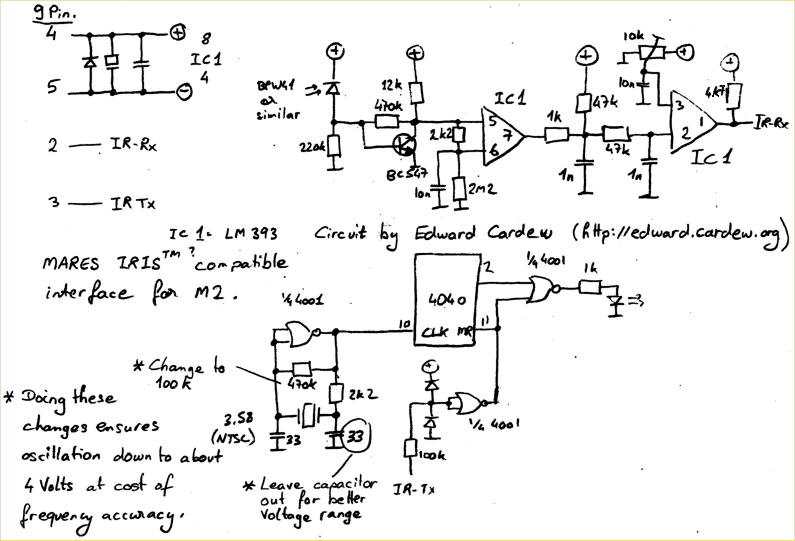
A TSOP4156 is often difficult to obtain or expensive to purchase. In response, an individual utilized old BPW41 infrared diodes to construct a custom receiver. The power source is derived from the RS232 port, requiring a minimum of 5.5...

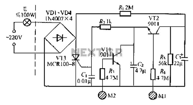
FIG IC, ICR, Ri, R, and AN composition form a bistable contact circuit with a Ge transistor. It includes components such as ICc, lc, c2, and Dj, and is associated with a one-shot delay circuit. The circuit can be...

The light-sensitive CDS cell R8 is configured in a bridge circuit with IC1 functioning as a comparator. When light strikes the CDS cell R8, the output of IC1 goes high, triggering SCR1. This action illuminates LED1 and activates opto...
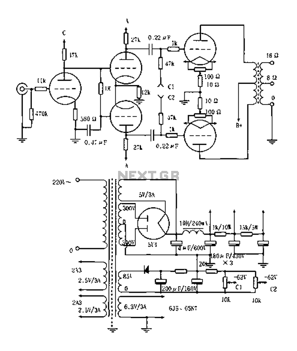
The Elliot 2A3PP line amplifier is a straightforward design, emphasizing the quality of the output transformer. It utilizes a 3KPP output transformer with a fixed bias of 62V, delivering an output power of 15W. The 2A3PP is well-suited for...