
How to Make a Simple 200 VA Homemade Power Inverter Circuit Square Wave Concept

The core of the inverter consists of a simple two-transistor astable multivibrator that generates the square wave signal. This signal is amplified by two medium-power Darlington transistors, which further drive the output stage comprising parallel-connected high-power transistors. These transistors convert the amplified square wave into high-current alternating pulses that are fed into the secondary windings of a power transformer. The induced voltage from the secondary to the primary winding results in a significant voltage conversion to either 230 or 120 volts, depending on the transformer specifications. The relatively weak square wave signals generated at the collectors of the transistors are applied to the bases of the driver transistors, also specified as Darlington pairs, which effectively amplify the signals to appropriate levels for the high-power output transistor configuration.
Upon receiving the signals from the driver transistors, the parallel output transistors saturate according to the varying signals, creating a substantial push-pull effect in the transformer's secondary windings. This alternating switching of the battery voltage through the windings induces a massive step-up power in the primary windings of the transformer, producing the desired AC output. Resistors placed at the emitters of the 2N3055 transistors, rated at 1 Ohm and 5 Watts, are included to prevent thermal runaway situations.
The most challenging component to procure may be the transformer, as a 10 Amp rated transformer is not commonly available. Alternatively, two 5 Amp rated transformers can be used, connecting their secondary taps in parallel. Another challenging aspect of the construction process is the fabrication of heat sinks. It is advisable to purchase ready-made heat sinks instead of attempting to make them, as this can be a tedious and time-consuming task. Various sizes are available on the market, and the appropriate ones should be selected, ensuring that holes are drilled correctly for the TO-3 package, which is the standard for the dimensions of power transistors like the 2N3055. The transistors should be securely attached to the heat sinks using 1/8 x 1/2 screws, nuts, and spring washers. It is possible to use either two separate heat sinks for the two sets of transistors or one large heat sink for the entire assembly.An efficiency of around 85 % and a power output of more than 200 watts is what you will get from the present design of a power inverter (home built). Complete circuit schematic and building procedure explained herein. You might have come across many articles regarding power inverters, however you might be still confused about making a power inverte
r The present content provides a complete building tutorial of a home built power inverter. If you are planning to make your own low cost and simple home built power inverter then probably you won`t find a better circuit than the present one. This heavy duty, easy to build design includes very few numbers of components which can be found readily available in any electronic retailer shop.
The output of the inverter will be obviously a square wave and also load dependent. But these drawbacks won`t matter much as long as sophisticated electronic equipment are not operated with it and the output is not over loaded. The big benefit of the present design is its simplicity, very low cost, high power output, 12 volt operation and low maintenance.
Besides, once it is built, an instant start is pretty assured. If at all any problem is encountered, troubleshooting won`t be a headache and may be traced within minutes. The efficiency of the system is also pretty high, in the vicinity of around 85% and the output power is above 200 watts.
A simple two transistor astable multivibrator forms the main square wave generator. The signal is suitably amplified by two current amplifier medium power Darlington transistors. This amplified square wave signal is further fed to the output stage comprising of parallel connected high power transistors. These transistors convert this signal into high current alternating pulses which is dumped into the secondary windings of the power transformer.
The induced voltage from the secondary to the primary winding, results a massive 230 or 120 volts conversion, as per transformer specifications. The relatively weak square wave signals generated at the collector of T1 and T2 is applied to the base of the driver transistors T2 and T3 respectively.
These are specified as Darlington pairs and thus very effectively amplify the signals to suitable levels so that they may be fed to the high power output transistor configuration. On receiving the signal from T2 and T3, all parallel output transistors saturate well enough according to the varying signal and create a huge push pull effect in the secondary windings on the power transformer.
This alternate switching of the entire battery voltage through the windings induce massive step up power into the primary windings of the transformer producing the desired AC output. The resistors placed at the emitter of the 2N3055 transistors are all 1 Ohm, 5 Watts and has been introduced to avoid thermal runaway situations with any of the transistors.
The only part of the circuit which is probably difficult to procure is the transformer, because a 10 Amp rated transformer is not easily available in the market. In that case you can get two 5 Amp rated transformers (easily available) and connect their secondary taps in parallel.
Next difficult stage in the building procedure is the making of the heat sinks. I won`t recommend you to fabricate them by yourself as the task can be quite a tedious one and time consuming too. It would be rather a better idea to get them ready made. You will find variety of them, in different sizes in the market. Select the suitable ones; make sure that the holes are appropriately drilled for the TO-3 package as shown in the figure.
TO-3 is the code to recognize typically the dimensions of power transistors which are categorized in the type used in the present circuit i. e. for 2N3055. Fix T5-T8 firmly over the heat sinks using 1/8 *1/2 screws, nuts and spring washers. You may use two separate heat sinks for the two sets of transistors or one single large 🔗 External reference
Related Circuits
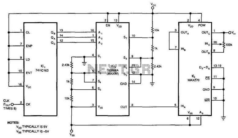
This circuit generates a pure sine wave with a total harmonic distortion (THD) of -80 dB and a frequency equal to the cutoff frequency (fc) of the filter in IC3. It utilizes a counter, an 8-channel analog multiplexer, and...

The image depicts a sine wave oscillator that consists of a quartz crystal (SJT) and gate A of the hex inverter IC CD4069. Compared to a standard RC phase-shift oscillator, the frequency stability of a crystal oscillator can achieve...

The image illustrates a circuit that utilizes a linear potentiometer (or linear Hall element) to control the PWM generation for two chassis drive motors in a gamepad or joystick used in model aircraft. J1 represents the handle of the...
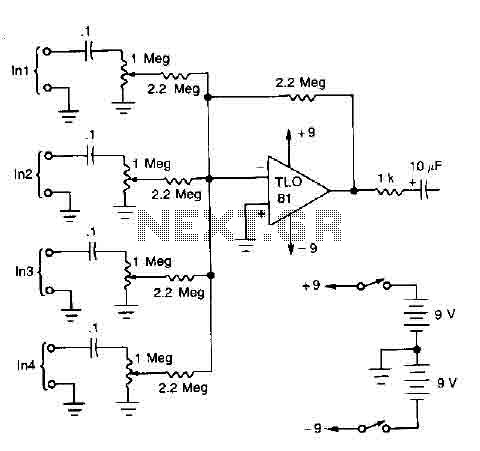
A TL081 operational amplifier is utilized as a high impedance to low impedance converter and as a signal mixer. The input impedance is approximately 1 megohm, while the output impedance is around 1 kohm. The circuit is powered by...

Before using LEDs, it is advisable to test them. An LED tester allows for testing even in low light conditions. LEDs are available in various shapes and colors, with some featuring clear, colorless packages and others having colored plastic...
It is essential to draw a circuit using a layout and conventions that are universally recognized. In electronic circuit design, adherence to standardized symbols and layout conventions is crucial for effective communication among engineers and technicians. A well-drawn schematic diagram...