
Hv739 Ultrasound Pulser Demo Board

The HV758DB1 demo board serves as an essential platform for evaluating the performance and capabilities of the HV758 high voltage pulse generator. The integration of high-speed level translators allows for compatibility with various logic levels, facilitating seamless interfacing with different control systems. The direct coupling method enhances the overall efficiency of the system by minimizing component count and simplifying the design, which is particularly advantageous in space-constrained applications.
The output capabilities of the HV758 are particularly noteworthy, with the ability to deliver significant peak currents suitable for driving capacitive loads. This feature is critical in ultrasound applications where rapid pulse generation is required to achieve high-resolution imaging. The flexibility of the HV758 in supporting both pulsing and continuous wave modes allows it to be utilized in a wide range of applications beyond ultrasound, including various types of transducer technologies.
The design considerations for PCB layout are also crucial, as the HV758's performance can be influenced by parasitic capacitances and inductances. Careful attention must be paid to the placement of components, routing of traces, and grounding practices to optimize the performance of the circuit. The built-in protection mechanisms further enhance the robustness of the system, ensuring that it can operate reliably under varying conditions.
Overall, the HV758DB1 demo board represents a versatile and high-performance solution for generating high voltage pulse waveforms, making it an invaluable tool for engineers and researchers in the field of ultrasound technology and beyond.This demo board data sheet describes how to use the HV758DB1 to generate the basic high voltage pulse waveform as an ultrasound transmitting pulser. The HV758 circuit uses the DC coupling method in all Level Translators There are no external coupling capacitors needed.
The VPP and VNN rail voltages CAN be changed rather quickly, compared to a high voltage capacitor gate- coupled driving pulser. This direct coupling topology of the Gate drivers not only saves two high voltage capacitors per channel, but also makes the PCB layout easier. The input stage of the HV758 has high-speed level translators that are able to operate with Logic signals of 1.
2V to 5. 0V and are optimized at 2. 5V to 3. 3V. In this demo board, the control Logic signals are connected to a high-speed ribbon cable connector. The control signal logic-high voltage should be the same as the VCC voltage of the demo board, and the logic-low should be referenced to GND. The HV758DB1 output waveforms CAN be displayed using an oscilloscope directly by connecting the scope probe to the test point TX1 to 4 and GND.
The soldering jumper CAN select whether or not to connect the on-board equivalent- load, a 330pF, 200V capacitor, parallel with a 2. 5k ©, 1W resistor. Also, a coaxial cable CAN be used to connect the user`s transducer to easily drive and evaluate the HV758 transmitter pulser.
The HV758 is a monolithic 4-channel, high-speed, high voltage, ultrasound transmitter pulser. This integrated, high performance circuit is in a single, 8x8mm, 64-Ball FCBGA package. The HV758 CAN deliver up to a ±2. 2A source and sink current to a capacitive transducer. It is designed for medical ultrasound imaging and ultrasound material NDT applications. It CAN also be used as a high voltage driver for other piezoelectric or capacitive MEMS transducers, or for ATE systems and pulse signal generators as a signal source. HV758 ½ ½s circuitry consists of controller Logic circuits, level translators, Gate driving Buffers and a high current and high voltage MOSFET output stage.
The output stages of each channel are designed to provide peak output currents over ±2. 5A for pulsing, when MC0 = 1 and MC1 = 1, with up to ±90V swings. When in mode 1, all the output stages drop the peak current to ±580mA for low-voltage CW mode operation to save power. Two‚oating 9VDC power supplies referenced to VPP and VNN supply the P- and N-type power FET Gate drivers.
The upper limit frequency of the pulser waveform is 20MHz depending on the load capacitance. One HV758 CAN also be used as four damping circuits to generate fast return-to-zero waveforms by working with another HV758 as four pulsing circuits. It also has built-in, under-voltage and over-temperature protection functions. 🔗 External reference
Related Circuits
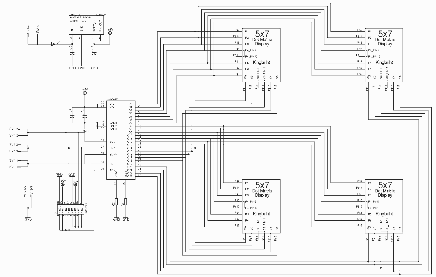
The MAX6953 from Dallas Maxim is a compact cathode-row display driver that interfaces a microprocessor (like PIC or AVR) to four 5x7 dot matrix LED displays through an I2C compatible serial interface. The chip includes some features that can...
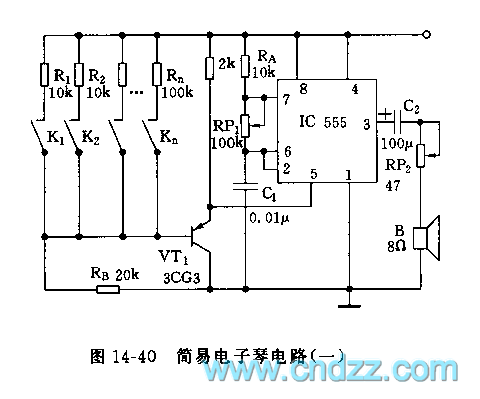
The controllable multivibrator, as illustrated in figure 14-40, consists of a 555 timer along with resistors RA, RP1, and capacitor C1. The oscillation frequency is influenced by the control voltage applied to pin 5. This control voltage is determined...
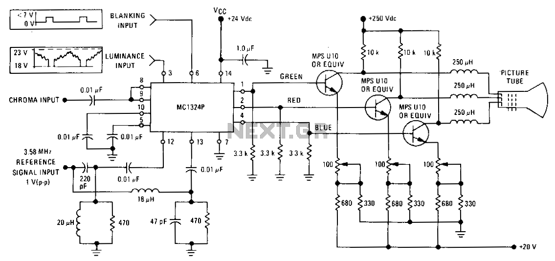
The MC1324 provides chroma demodulation, recovering the R, G, and B signals to drive video amplifiers for each color difference signal. The luminance signal and chrominance signal are matrixed to obtain the R, G, and B signals. The MC1324 is...
The expansion board had six servo ports, but the cost did not justify the number of ports. A modification was made to the handyboard, allowing for a total of 16 servo ports at a minimal cost of approximately $2,...
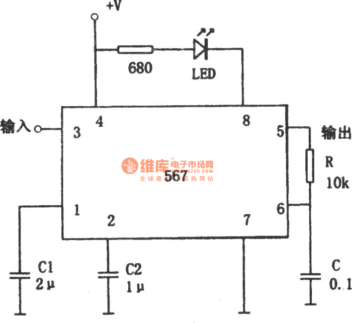
The circuit depicted in the figure is a 567 FM demodulation circuit. The FM signal enters through pin 3, and the demodulated output signal is available at pin 5. The center frequency of the FM signal that the circuit...
Instructions for constructing a circuit on veroboard by interpreting the schematic. Experienced constructors can directly reference the schematic to begin assembly, utilizing their knowledge of component placement and efficient use of veroboard space. Beginners should have certain foundational skills,...