
Hybrid power amplifier 01

The CD4069 is a hex inverter, featuring six independent inverting gates, which can be used to implement various digital logic functions. The structure of the CD4069 is based on complementary metal-oxide-semiconductor (CMOS) technology, which allows for low power consumption and high noise immunity. The CMOSFET configuration enables the device to maintain a high input impedance, making it suitable for interfacing with various signal sources without loading them down.
The input-output characteristics of the CD4069 exhibit a sharp transition between the high and low states, resulting in a superior switching performance. This characteristic is particularly beneficial in applications requiring precise timing and signal integrity, such as in clock generation and pulse modulation circuits. The idealized characteristic curve demonstrates the expected performance under optimal conditions, while the actual characteristic curve illustrates real-world behavior, including the linear region that can be exploited for amplification purposes.
In the application depicted in Figure 2-5 (d), the CD4069 is configured as an audio amplifier. The input audio signal, designated as ei, is fed into one of the inverting gates. The configuration enhances the input signal, producing a high-fidelity output signal, eo. This amplification capability allows the CD4069 to be effectively used in audio processing applications, ensuring that the output signal retains the quality and characteristics of the original input.
Overall, the CD4069 is a versatile component suitable for a wide range of applications, from digital logic circuits to analog signal processing, owing to its robust performance and adaptable nature in various configurations. CD4069 unit structure of FIG. 2-5 (a) shown below, it is composed of two abutment surfaces into CMOSFET, the input-output characteristics shown in Figure 2-s (b) in Fig. Becaus e of its characteristics is a superior unit switching curve, so a combination of common CD406q into various types of automatic switch control circuit, a single spike or square cross generator, in fact, seldom as a linear amplifier 6 Figure 2-5 (b) of the the curve shown is idealized characteristic line, the actual characteristic curve shown in Figure 2-5 (c) as shown, there is a linear zone in its middle region. As a result the unit CD4069 are connected in FIG. 2-5 (d) an amplifier in the form shown in the CD4069 input audio signal injection time signal ei, at its output can be made of high-fidelity amplified signal eo,
Related Circuits
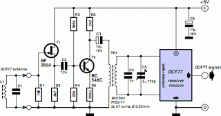
A popular project among microcontroller enthusiasts is to construct a radio-controlled clock. Compact receiver boards are available, equipped with a pre-tuned ferrite antenna, which can receive and demodulate the DCF77 time signal broadcast from Mainflingen, Germany. The DCF77 signal...
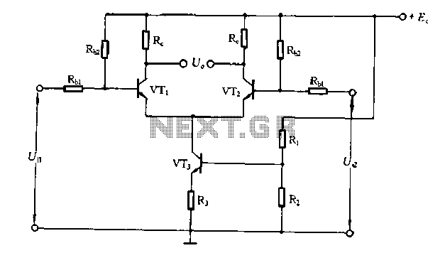
The differential amplifier circuit features a constant current source. The differential amplifier is a fundamental building block in analog electronics, utilized for amplifying the difference between two input voltages while rejecting any signals that are common to both inputs. Central...
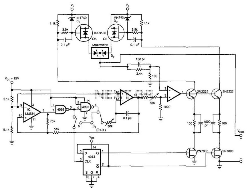
This power booster operates as a high-efficiency power multiplexer or, when supplied with an external signal source, as a high-power linear amplifier. For driving a load with a high-power square wave, the circuit alternately draws power from two external...
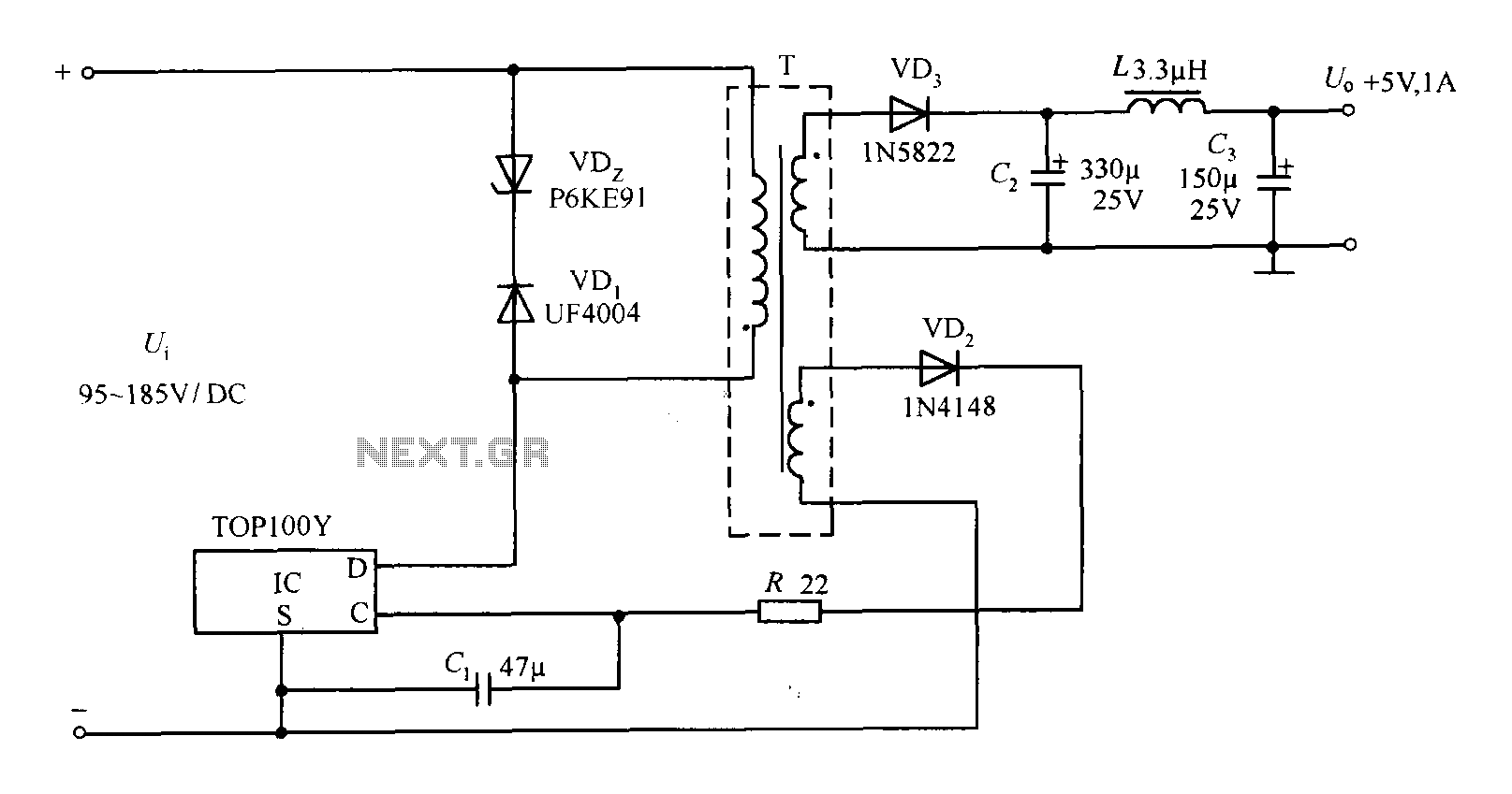
The TOP100Y is a flyback DC switching power supply circuit with a +5V, 1A output. This power supply features a feedback circuit that directly regulates the output voltage, making it suitable for applications that require electrical isolation and minimal...
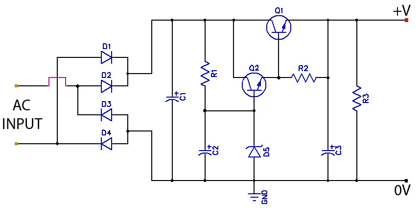
The value of capacitor C2 can be selected to achieve the desired level of smoothness, as its capacitance is effectively amplified by the combined gains of transistors Q1 and Q2. For instance, if a capacitance of 100 µF is...
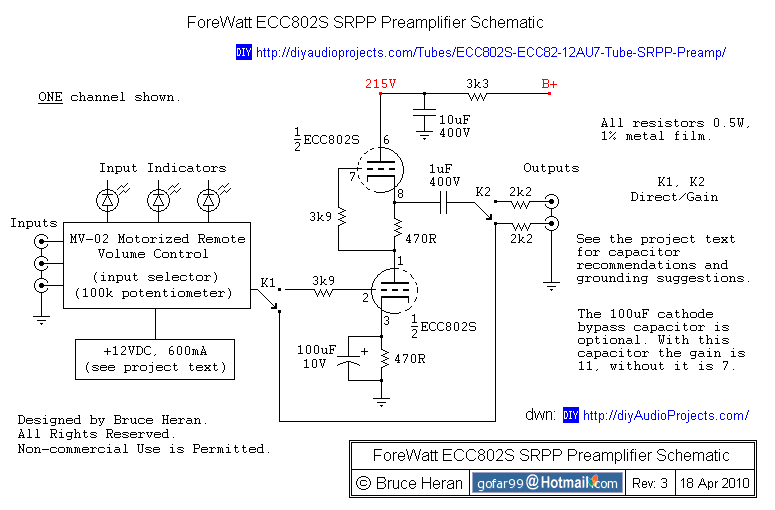
The project involves a shunt-regulated push-pull (SRPP) driver stage. Research and modeling have been conducted on the SRPP, highlighting its advantages, which include good linearity, low distortion, low output impedance, effective power supply noise rejection, and moderate gain. The...