
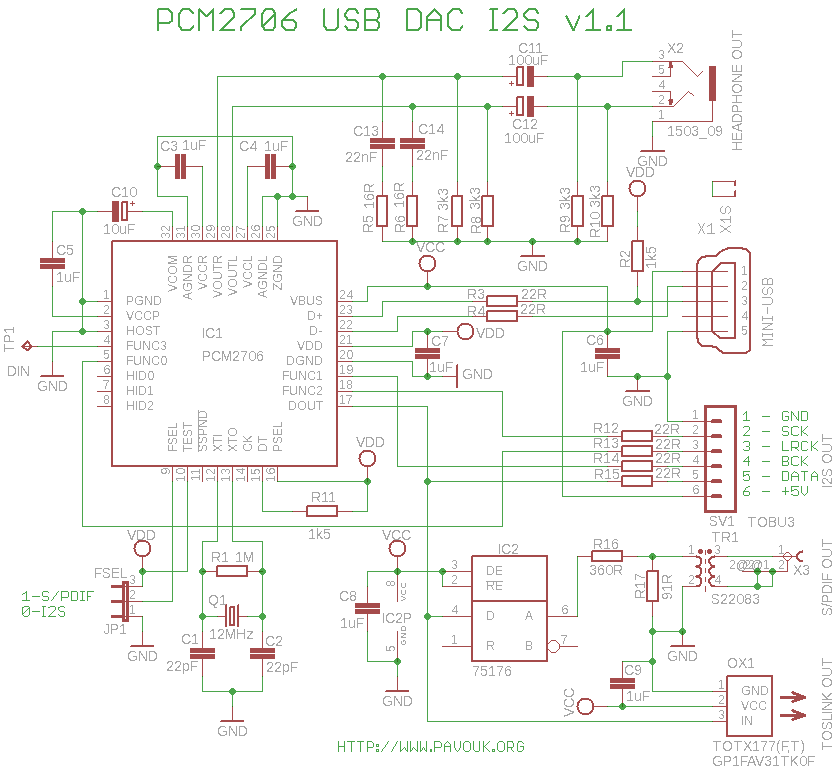
I2S isolator

The described circuit is a critical component in ensuring the integrity and quality of the audio signal processed by the DAC. The galvanic isolation provided by the IL715E integrated circuit effectively prevents ground loops that could introduce noise into the audio signal. The dual power supply configuration allows for stable operation of both the input and output sides of the isolator, which is essential for maintaining the fidelity of the digital audio signal.
The choice of inductors and capacitors around the DC/DC converter is crucial for filtering out noise and ensuring that the power supply to the isolator is clean and stable. The specified load resistor R1 ensures that the converter operates within its optimal current range, thus preventing any potential underperformance due to insufficient load.
The design considerations for the PCB layout are also noteworthy. By positioning the components on the opposite side of the board from the DAC, the risk of interference is minimized, ensuring that the DAC can perform at its highest quality without degradation from nearby components. The use of right-angle connectors further enhances the usability of the design, allowing for a compact assembly while ensuring that the connections remain secure and accessible.
Overall, this circuit design is an effective solution for achieving high-quality audio output from a DAC while maintaining isolation from potential interference sources, thereby enhancing the overall performance of the audio system.To avoid hum and interference in our high quality DAC we need to galvanically isolate him from a signal source and break potential unwanted ground loop. One possibility is to isolate DAC on input of the S/PDIF decoder with pulse transformer or connect him with optical TOSLINK.
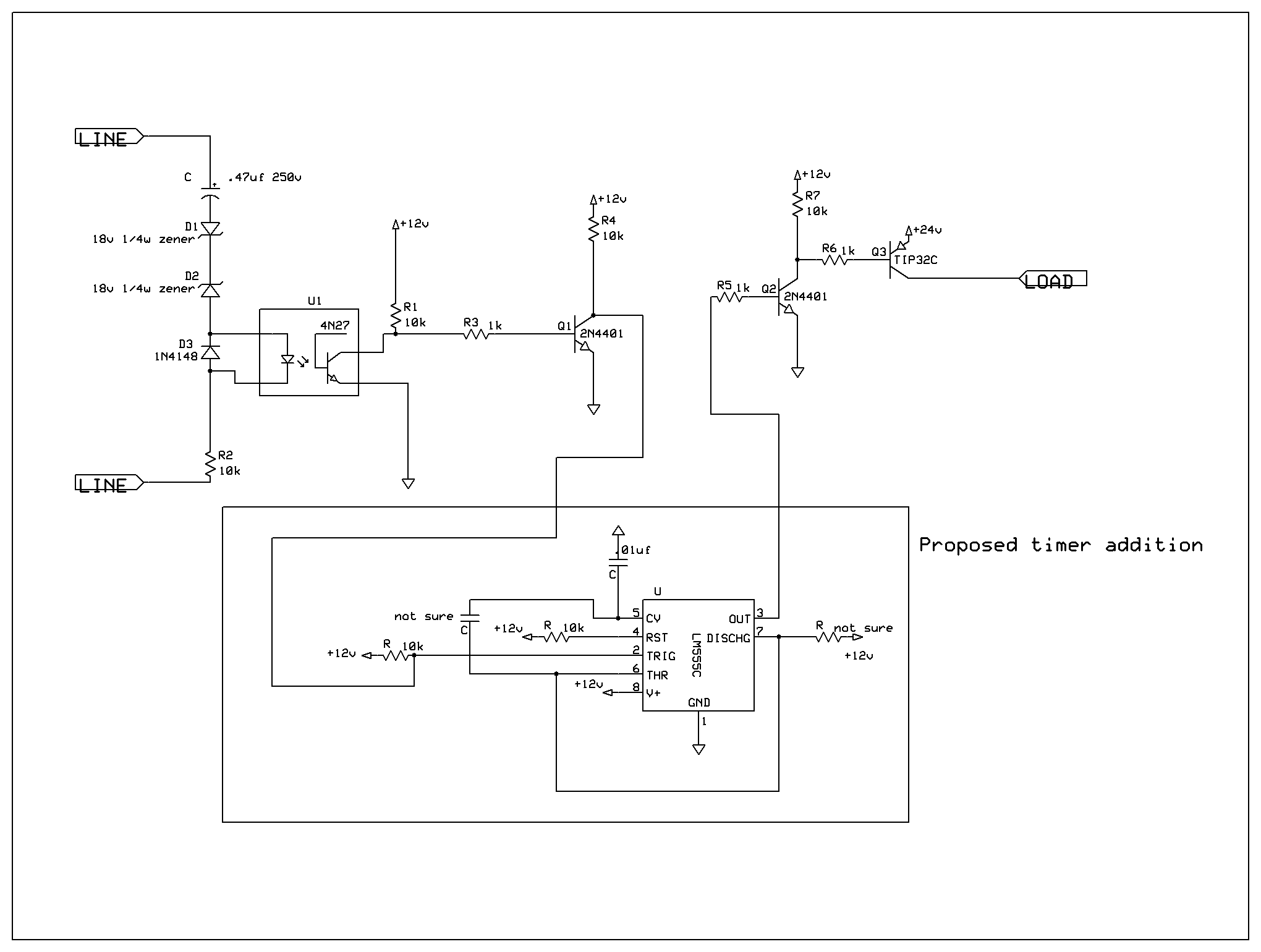
When we want to connect DAC directly from USB receiver via I2S bus, tha t we must use special integrated circuit which works like electrical isolator of TTL signals. Circuit use specialised circuit IL715E which have on the one side four TTL inputs and on the opposite side corresponding outputs. It perfectly fits to I2S bus, where we have DATA, BCK, LRCK and SCK signals. Circuit requires dual supplying, one on the input and second on the output side. On the input is supply connected to +5V which I bring out them on the I2S connector for future use. Secondary side is supplied from small DC/DC converter. According to recommendations are around converter inductors L1 and L2 and filter and block capacitors.
Their values correspond to changer from Aimtec company but probably parts will be acceptable for changers from other companies. For reliable function of converter is on the secondary side load resistor R1 which guarantee minimal current consumption about 20mA.
Datasheet have informations about maximum data rate 100Mbps which is far away from our sample frequency 48kHz, where frequency of BCK is 3. 072MHz and SCK is 12. 288MHz with 4x oversampling. Circuit should work with 192kHz/24bit samples where frequency of SCK is higher 49. 152MHz. DAC without oversampling doesn`t use SCK signal that we must care only maximal BCK frequency. It is possible to use isolators from other vendors with same pinout, but we must check their maximum data rate and if they doesn`t need ENABLE signal.
First we solder integrated circuit and next other SMD components. Last we solder converter and converter from the other side. We must be careful for right orientation of circuit and changer and right polarity of capacitors. If we use circuit which requires ENABLE signal on the pin 10 that we join SJ1. PCB is designed single-sided. Be careful that board is placed between decoder and DAC board up side down. It means that SMD components from a bottom side will be visible up and socket ribbons will be connected to the pins of neighbor boards. First version of board, which I designed had components on the side, where is big filter capacitor on a DAC board, that it was not possible to directly plug board to the neighbours.
This version of board has components on the opposite side that it doesn`t collide with parts on the DAC board. It is possible to use right angle connectors where we will not have troubles with space, but boards will need much place.
🔗 External reference
Related Circuits

An RF isolator is a seemingly magic device that allows signals to pass in only one direction. Signals applied to the input port are sent to the test port and signals coming into the test port can only go...
This project involves a couple of USB Digital-to-Analog Converters (DACs) that lack I2S output. Some users do not require S/PDIF input and prefer a direct USB connection. Therefore, it is unnecessary to convert the signal from USB to S/PDIF...
A ground loop in your AV system caused by antenna connection or TV cable is very common if you have your computer connected to the same system. This type of ground loop problem can be solved by using suitable...
This is a circuit to use a standard, low quality opto isolator to transfer an analogue signal with reasonable linearity and without complicated feedback loops to monitor and linearise it. The circuit was designed to interface a mains driven...
This circuit is useful for removing ground loop hum on a remote line level audio signal line. It can be used to connect a computer sound card to a stereo amplifier's line input. Other uses include tapping into a...
A ringer interface circuit is designed to buffer the output of a central telephone system, which connects to multiple ringers distributed throughout a building. This circuit addresses an issue where the line overloads when ringing, requiring a reset. The...