
IC CA3140 Datasheet

The CA3140 operational amplifier is designed to provide high-speed performance while maintaining low power consumption, making it suitable for a variety of applications. Its BiMOS architecture combines the high input impedance characteristics of MOSFETs with the low output impedance and high current drive capability of bipolar transistors. This unique combination allows the CA3140 to operate effectively in both analog and digital circuits.
The amplifier operates with a supply voltage range from ±3V to ±15V, providing versatility for different circuit designs. With a gain bandwidth product of 4.5 MHz, the CA3140 is capable of handling high-frequency signals, making it ideal for applications such as audio processing, signal conditioning, and active filtering.
The input stage, utilizing MOSFET technology, offers a very high input impedance, which minimizes the loading effect on preceding stages. This is particularly advantageous in sensor applications where signal integrity is critical. The bipolar output stage ensures robust drive capability, allowing the amplifier to interface with a wide range of loads without distortion.
In terms of performance specifications, the CA3140 boasts a slew rate of 13 V/µs, enabling it to respond quickly to rapid changes in input signals. Additionally, the device features low noise characteristics, which is essential for precision applications. The output can swing close to the supply rails, providing maximum output voltage range and making it suitable for single-supply operation.
Overall, the CA3140 operational amplifier is a versatile component that combines high performance with ease of use, making it a popular choice among engineers for various electronic applications.CA3140 is the 4.5MHz BiMOS Operational Amplifier with MOSFET inputs and Bipolar output. This Op Amp combines the advantage of PMOS transistors and high vol.. 🔗 External reference
Related Circuits
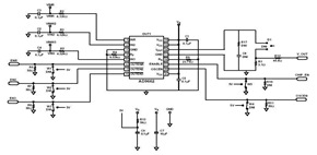
This schematic was created using a 2-layer evaluation board for the AD9662 3-Channel Laser Diode Driver. This device is primarily utilized in high-performance CD-DVD recordable drives and for laser diode current switching. The AD9662 is a specialized integrated circuit designed...
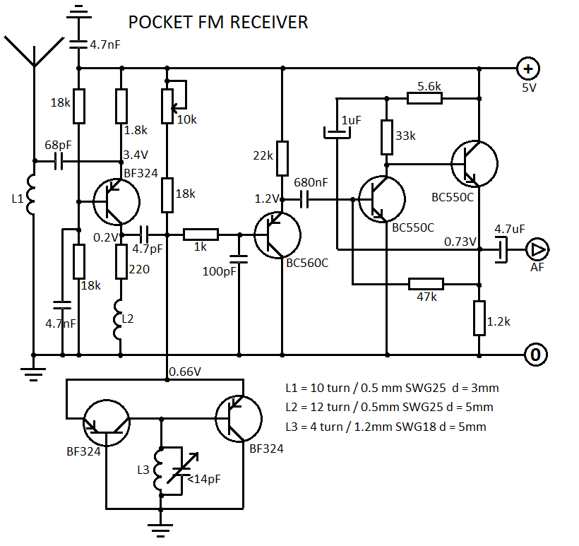
TCA440 is an AM receiver circuit designed for long wave (LW), medium wave (MW), and short wave (SW) applications in both battery-operated and line-operated radio receivers. It features an RF pre-stage with automatic gain control (AGC), a balanced mixer,...
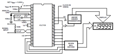
The schematic below shows the ICL7135 integrating analog-to-digital converter (ADC) functional diagram. According to the datasheet, an integrating converter is the right choice for panel meters and digital voltmeter applications. It can also be used for reducing line frequency...
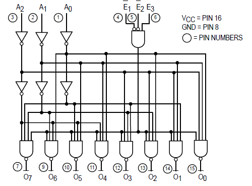
The Motorola SN54/74LS138 is recognized as a 1-of-8 decoder or demultiplexer, specifically engineered for high-speed bar memory chip select address decoding. The accompanying diagram illustrates the logic configuration of the SN54/74LS138 demultiplexer. According to the SN54 datasheet, the multiple...
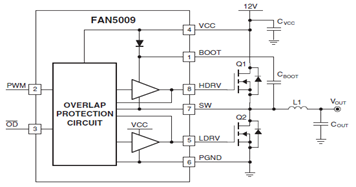
The schematic illustrates a typical application circuit for the FAN5009, a dual bootstrapped 12V high-frequency MOSFET driver. When integrated with a multi-phase PWM controller and power MOSFETs, it can form a complete core voltage regulator for microprocessors, as specified...
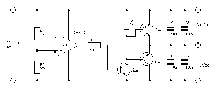
Another circuit for a balanced diet from a single voltage network. In fact, this is a uitbreding the other voltage divider circuit using a some power darling tons as buffer. This buffer can deliver a 200 to 300 mA....