
Improved one-shot timer circuit composed of 2 PUT

The improved trigger timing circuit is designed to provide precise control over timing applications. The circuit's functionality begins when a set signal is applied to the input, which initiates the conduction of VT1. This conduction allows current to flow through the relay K, effectively energizing it and enabling its contacts to close, thus providing power to the subsequent components in the circuit.
Simultaneously, the charging process of capacitor C1 begins. The charging rate of C1 is determined by the resistor-capacitor (RC) time constant, which dictates how quickly the capacitor reaches a certain voltage level. As C1 charges, it provides a stable voltage to PUT1, allowing it to turn on once the voltage across it exceeds its threshold. The interaction between C1 and PUT1 is critical, as it sets the timing for the entire circuit operation.
The use of two PUTs enhances the circuit's performance by allowing for more precise control over the timing intervals. The first PUT can be configured to respond to the voltage across C1, while the second PUT can be used to manage the discharge cycle, ensuring that the timing sequence is both reliable and adjustable. The overall design of the circuit provides flexibility in applications such as delay timers, pulse generators, and other timing-related functions in electronic systems.
In summary, this improved trigger timing circuit effectively integrates the characteristics of PUTs and capacitors to create a robust timing solution, capable of delivering accurate and repeatable results in various electronic applications.Figure 1 is an improved trigger timing circuit composed of 2 PUT. If you add the set signal, the circuit will be set, transistor VT1 turn to the conduction state, the relay K will be energized action. It supplies voltage for the delay voltage at the same time. Therefore, the capacitor is charged by C1. PUT1 is conducted by positive voltage. C1 passes PUT1,.. 🔗 External reference
Related Circuits

A 2 x 18W Hi-Fi Stereo Power Amplifier is designed using two TDA2030 integrated circuits (ICs). This amplifier features good input sensitivity, low distortion, stable operation, and comprehensive protection against overloads and output short-circuits. It can serve as a...
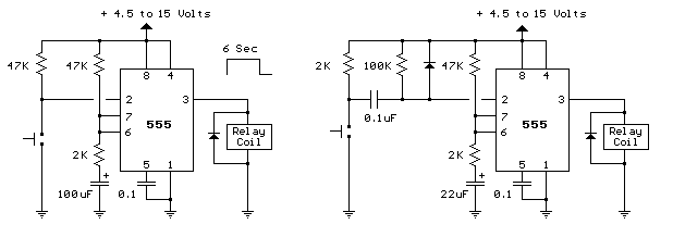
The two circuits below illustrate using the 555 timer to close a relay for a predetermined amount of time by pressing a momentary N/O push button. The circuit on the left can be used for long time periods where...

Fixed-value capacitors are disc ceramics. C1, C4, C5, C6, and C8 are NPO ceramic or polystyrene. C2 is a 25-pF ceramic trimmer and C3 is a 15-pF miniature air variable capacitor. The resistors are ¼ watt carbon film or...
The diagram illustrates a human infrared remote sensing lamp circuit. It utilizes the trace infrared heat emitted by humans to control the lamp's operation, allowing it to turn on or off remotely. This human infrared remote sensing lamp features...
The PGA103 is designed with a wide input voltage range. It utilizes a voltage divider circuit consisting of a 11.3kΩ resistor and a 102kΩ resistor, achieving a division ratio of approximately 1/10. For instance, when the input voltage is...
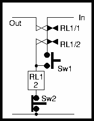
Probably the easiest way of doing automatic switch off is with relay logic. In the diagram, the box marked RL1 is the coil, the 2 in the coil box tells you there are two sets of contacts somewhere on...