
Infinite sample and hold amplifier

The described circuit operates on the principles of sample-and-hold technology, which is crucial in analog-to-digital conversion processes. The S/H amplifier serves as a critical component in maintaining signal integrity during the conversion cycle. In normal operation, the S/H amplifier buffers the analog voltage, ensuring that the output reflects the input accurately. When the SAMPLE signal is activated, the S/H amplifier transitions to hold mode, effectively freezing the output voltage. This is essential for preventing any fluctuations in the output during the conversion process, which could lead to inaccuracies.
The input sample-and-hold amplifier is responsible for capturing the latest analog voltage. This action is synchronized with the SAMPLE signal, ensuring that the most current voltage is held stable for conversion. The SAR D/A converter plays a pivotal role in adjusting the output to match the new input voltage, continuously refining its output to minimize discrepancies between the actual and desired voltages.
Once the conversion is complete, the output S/H amplifier reverts to track mode, allowing it to follow the new analog voltage. This transition is critical as it enables the system to adapt to changes in the input signal, maintaining accuracy and responsiveness in real-time applications. Overall, the circuit's design emphasizes precision and reliability, making it suitable for various applications in signal processing and digital communication systems.During normal' 'hold'' mode, the replicated analog voltage is buffered straight through the S/H amplifier to the output. Upon issuance of a SAMPLE signal, the S/H amplifier is placed in the hold mode, holding the voltage until the new analog voltage is valid.
The same SAMPLE signal triggers an update to the input sample-and-hold amplifier. The most current analog voltage is captured and held for conversion. The previously determined voltage is held stable at the output during the conversion cycle while the SAR/D-to-A converter continuously adjusts to replicate the new input voltage. At the end of the conversion, the output sample-and-hold amplifier is once again placed in the track mode. The new analog voltage is then regenerated.
Related Circuits
The schematic diagram presented is of a twin "T" phase shift oscillator, an audio oscillator. This oscillator derives its name from the phase shift network formed by resistors R3, R4, and capacitors C1, C2, and C3. This network shifts...
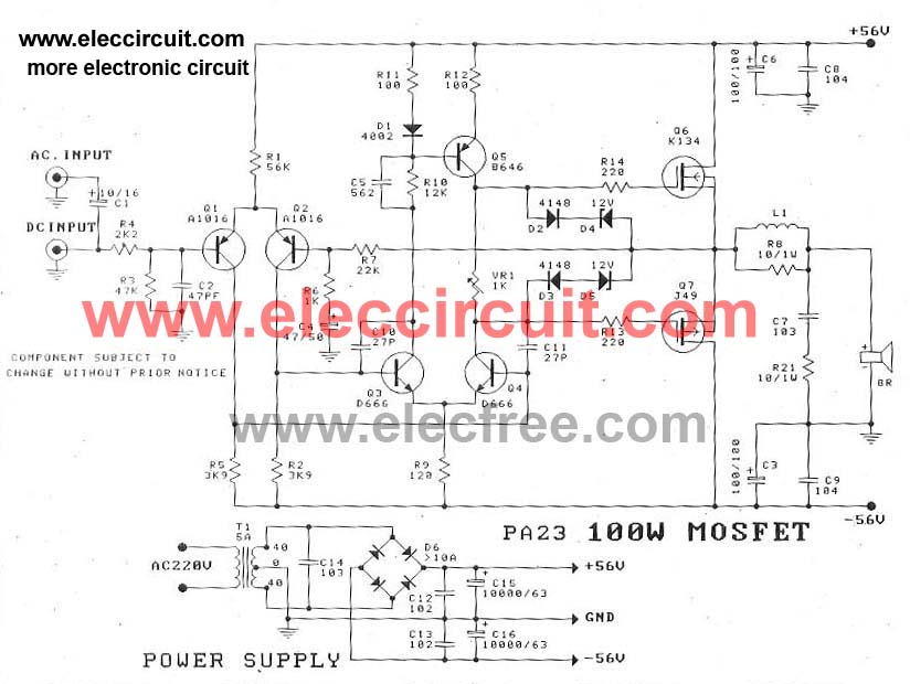
This circuit is a MOSFET power amplifier configured in an OCL (Output Capacitor-Less) topology. It delivers an output power of 100 watts and can utilize MOSFETs such as K134 and J49 or J162 and K1058. When driving an 8-ohm...
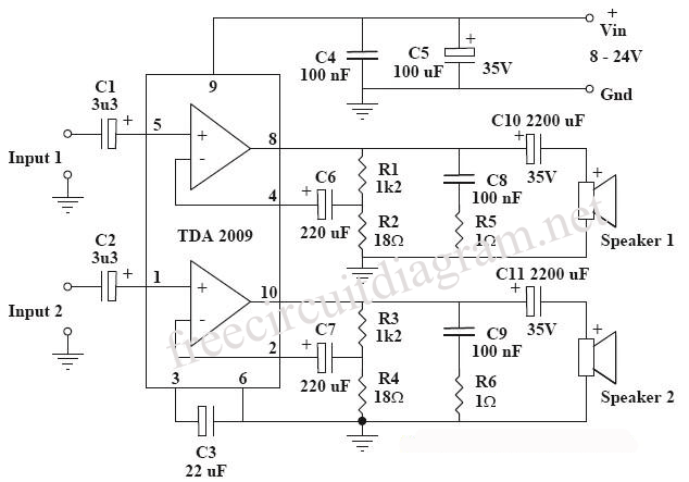
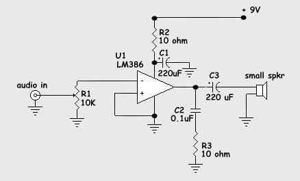
This circuit is a diagram of a mini amplifier. The amplifier circuit has a power output of 10 watts and is well-suited for car audio applications. It utilizes the TDA2009A integrated circuit as the power amplifier. To prevent excessive...

In a single difference amplifier configuration, the AM-427 demonstrates excellent common-mode rejection and low noise voltage, which is primarily influenced by the resistor Johnson noise. The three-amplifier configuration presented circumvents the low input-impedance characteristics typical of difference amplifiers. Due...
The following circuit illustrates a power supply for an amplifier circuit diagram. Features include ease of construction and adequate electrical response. The power supply circuit for an amplifier is a crucial component that ensures the amplifier operates effectively. It typically...
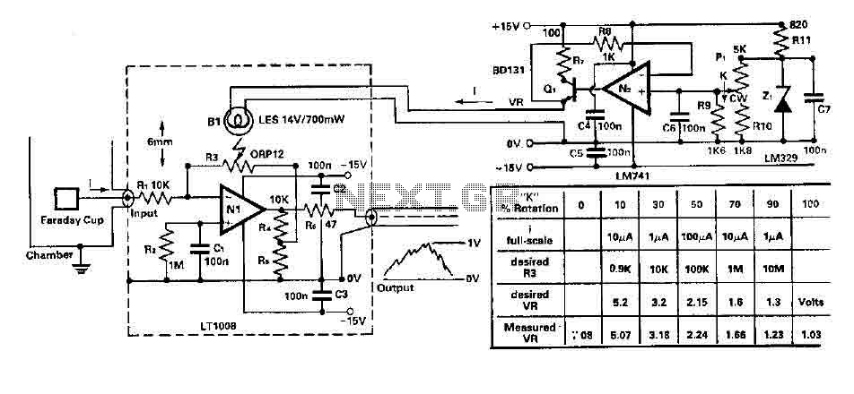
To amplify small current signals as an electron collector inside a vacuum chamber, it is advantageous for reasons related to noise and bandwidth to have a "head-amplifier" connected to the chamber. Operational amplifier 1 is a precision device featuring...