
integrated circuit Wiring a 74LS259 (addressable latch)
")
The 74LS259 is an 8-bit addressable latch that is commonly used in digital circuits for storing binary data. It features eight data inputs (D0 to D7), an address input (A0 to A2), a latch enable input (LE), and an output enable input (OE). The device operates on a positive logic level and is typically powered by a +5V supply.
To configure the 74LS259, the first step involves connecting the power supply. The Vcc pin should be connected to +5V, while the ground (GND) pin should be connected to the system ground. The data inputs (D0 to D7) can be connected to various digital signal sources, such as switches or other logic devices, which will provide the binary data to be latched.
The address inputs (A0 to A2) are used to select which of the eight data inputs will be latched. These inputs should be connected to a binary counter or manually set to select the desired input. The latch enable (LE) input must be driven high to allow data to be latched. When LE is low, the output will retain the last latched value.
The output enable (OE) input, when driven low, allows the latched data to be output on the Q0 to Q7 pins. If OE is high, the outputs will be in a high-impedance state, effectively disconnecting them from the circuit. This feature is useful for multiplexing applications where multiple devices share the same output lines.
For testing purposes, a simple circuit can be set up with push buttons connected to the data inputs and a binary counter connected to the address lines. By pressing the buttons, different binary values can be latched, and the corresponding output can be monitored. This approach allows for a comprehensive understanding of the latch's operation without requiring a microcontroller, providing a clear insight into the device's functionality and behavior in a digital circuit.I`m trying to use a 74LS259 8 bit addressable latch. I`m trying to get it working without a micro-controller first to ensure that I understanding the wiring 100%. 🔗 External reference
Related Circuits
A new user has recently discovered a Laser Alarm System and has decided to explore this project. The Laser Alarm System is a security device that utilizes laser beams to detect unauthorized entry or movement within a designated area. The...
A simple audio amplifier with a 10 Vpp output designed for use with the AD633 ring modulation chip. The datasheet for the chip is available, and the circuit will utilize the XR2206 function generator IC for the modulation input....
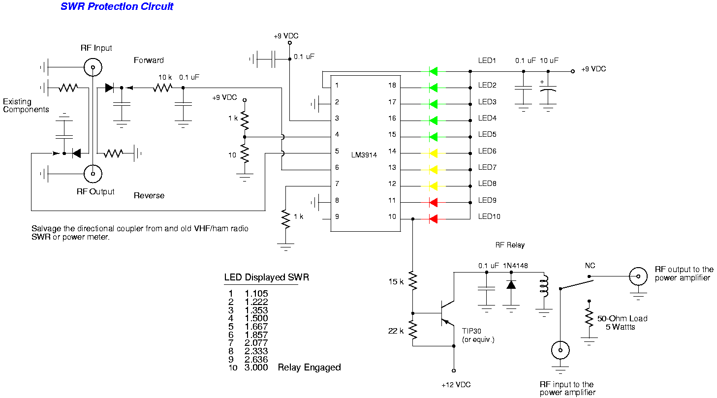
This scheme is a Standing Wave Ratio (SWR) meter, which is relatively simple and can be easily constructed. Once a directional coupler is created, the results will be indicated on the measuring LED meters as a ratio of SWR. The...
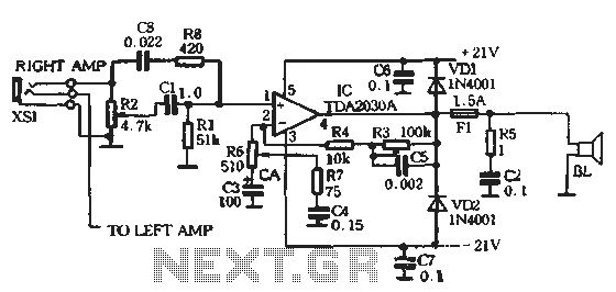
The circuit comprises two main components: the Lisheng power amplifier and the rectifier filter section. The stereo audio power amplifier circuit diagram, depicted in Figure 5-85, illustrates only one channel, with the other channel being identical. The audio signal...

This is a single-zone alarm system featuring automatic exit, entry, and siren cut-off timers. It is designed to accommodate various types of normally-closed input devices, including magnetic reed contacts, foil tape, and passive infrared sensors (PIRs). Additionally, it is...
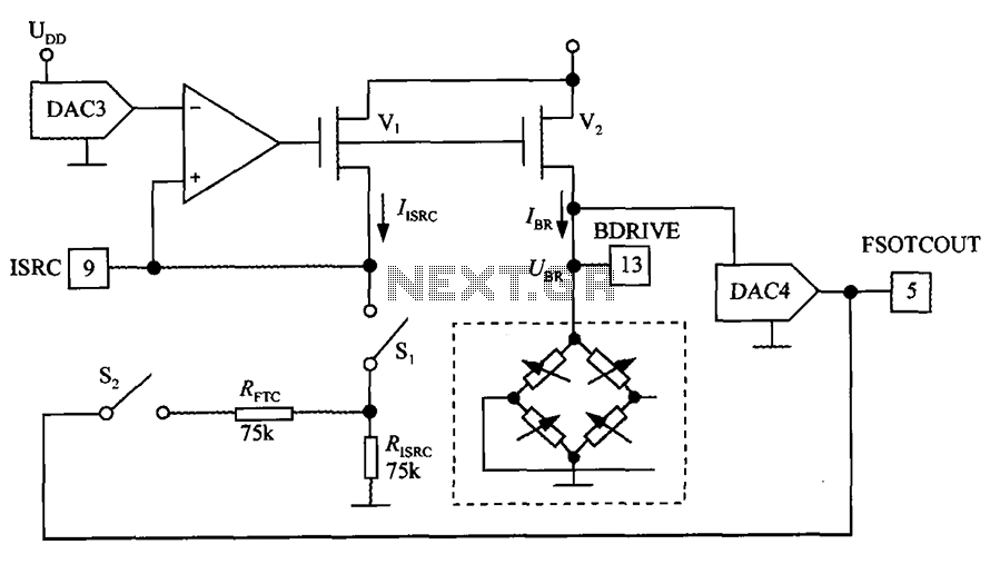
The excitation circuit for the digital pressure signal conditioner MAX1458 is illustrated. The output DAC3 is utilized to adjust the sensor excitation current (IBR), enabling full-scale fine calibration. The reference current (IISRC) is determined by the resistor RISRC and...