
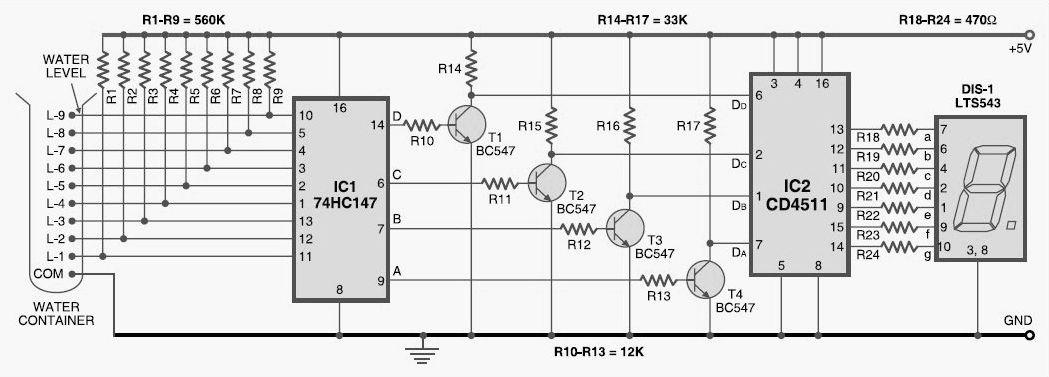
intercom circuit

This intercom circuit operates effectively with minimal components, demonstrating the efficiency of using three transistors in its design. The primary function of the circuit is to generate ringing signals when switch S2 is activated, allowing for communication between two or more stations.
The circuit can be divided into two main sections: the transmitter and the receiver. Each section employs one transistor for amplification and two additional transistors for signal processing and switching. The transistors are typically configured in a common emitter arrangement, which provides the necessary gain for the audio signals.
For a two-way intercom system, two identical circuits are required. Each circuit can be connected to a common power supply and linked via audio lines, allowing for seamless communication. The intercom can be enhanced with additional features such as volume control, which can be implemented using variable resistors in the audio path.
Current consumption is an important factor in the design, especially for battery-operated systems. The transistors should be selected based on their low quiescent current characteristics to ensure the circuit remains energy-efficient. When designing the layout, careful consideration should be given to component placement to minimize noise and ensure clear audio quality.
In summary, this intercom circuit design is not only straightforward and cost-effective but also scalable, allowing for multiple intercom stations to be added as needed while maintaining high audio fidelity and low power consumption.A very good quality and simple intercom circuit using only three transistors. By pressing the switch S2 the circuit will generate ring signals. For making two way intercom make two identical circuits and combine them as shown in diagram 2. The current consumption of the circuit 🔗 External reference
Related Circuits
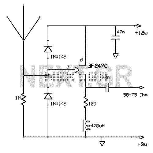
This active antenna schematic can be used to frequency range from 10 KHz to 100 MHz. The length of the Antenna can be between 0.5 to 1 meter long. The power consumption is 20-30mA. More: Use the shortest possible...
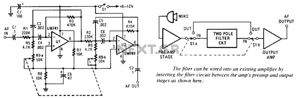
This variable-frequency audio bandpass filter is constructed using two 741 operational amplifiers (op amps) connected in cascade. Both op amps are configured as identical RC active filters, enhancing the selectivity of the overall circuit. The filter has a tuning...
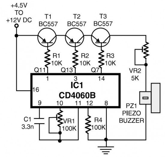
The circuit generates pulses of 1.25 Hz from pin 1 and 20 Hz from pin 14. The three output pins of IC1 are connected to the base terminals of transistors T1, T2, and T3 through resistors R1, R2, and...
A printed circuit board (PCB) was presented along with a schematic detailing the arrangement of components required for the activation of an LED on the board. The purpose of the PCB is to facilitate planning for the eventual construction...
A simple tool to check the degree of radiation from an electric or electronic instrument. The LEDs in the circuit will provide a running light pattern when the circuit detects electromagnetic radiation from the device. It can identify radiation...
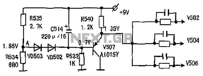
The common-emitter amplifier circuit V502, V504, V506 is designed to generate a static potential bias voltage through an emitter follower configuration, as illustrated in Figure 3. The active filter is formed by components V507, VD502, and VD503. The emitter...