
Internal functional block diagram of NCP5201

The NCP5201 is designed to efficiently manage power conversion through the use of pulse width modulation (PWM) techniques. The chip operates by generating two sets of PWM signals that are out of phase, allowing for efficient control of the field effect transistors (FETs). The alternating operation of the FETs ensures that the battery supply voltage is effectively transformed into a pulsed output, which is crucial for applications that require a stable voltage supply.
In the first stage, the PWM signals control the gates of the FETs, enabling them to switch on and off rapidly. This switching action is what allows the circuit to convert the DC battery voltage into a pulsed output. The inductor L2 and capacitor COUT play a vital role in smoothing out the pulsed voltage, resulting in a stable +2.5 V output. This voltage is essential for the operation of memory circuits, which often require a specific voltage level for optimal performance.
Furthermore, the internal circuitry of the NCP5201 utilizes the +2.5 V supply to power a second PWM generation circuit. This circuit operates similarly to the first, utilizing two additional FETs to produce another pulsed output signal. The output from this second stage is filtered through capacitors C14, C15, and C16, which work together to reduce ripple and provide a clean 1.25 V DC output. This lower voltage is typically used to power memory devices that require a reduced voltage level.
Overall, the design of the NCP5201 chip exemplifies the integration of multiple power management functions into a single component, allowing for compact and efficient circuit designs in electronic applications.Having two sets of PWM signal generating circuit within NCP5201 chip, a set of output pins and the feet two opposite phase PWM signal, respectively applied to the gates of the three field effect transistor, the field effect transistor so that two sets are alternately turned on the battery supply voltage into a pulse voltage, then by L2, COUT filter becomes +2.5 V voltage supply for the memory. At the same time, + 2.5 V power supply is applied to the chip @ foot inside the chip provided with a second set PWM signal generating circuit and two field-effect transistors.
The two field effect transistors of the voltage of 2.5 V into a pulse signal, pin output by the chip, the C14, c15, C16 after filtered output DC voltage 1.25 V, power the circuit memory.
Related Circuits
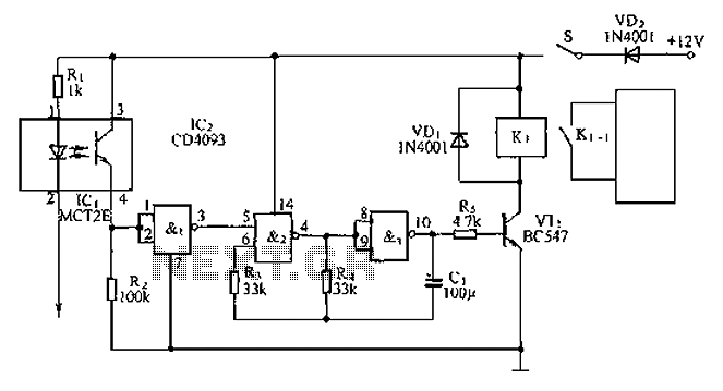
An anti-theft car audio system circuit is depicted, powered by a 12V DC supply from the car battery. Upon closing switch S1, the light-emitting diode in optocoupler IC1 activates, causing the phototransistor to conduct. This results in a high-level...
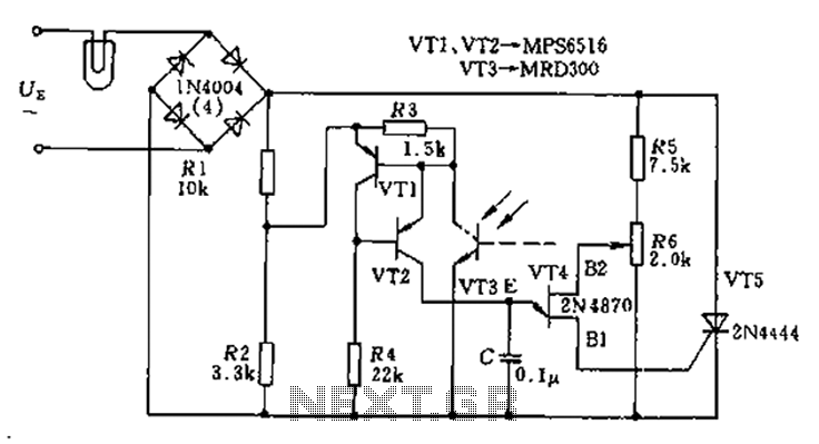
The circuit utilizes a thyristor-based AC automatic voltage regulator to stabilize the brightness of lamp L. A diagonal line connects the thyristor to the T5 bridge. The trigger pulse for the thyristor is generated by a single-junction transistor, VT4....
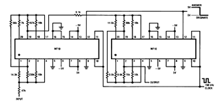
Later, there will be applications including a Basic Circuit Description, Block Diagram of the MF10, Programmable Dual Clock Generator, Butterworth Lowpass Filter, MF10 as an Input Filter and Sample/Hold, Generating Quadrature Sine Waves, and the Non-Inverting Integrator used in...

The automotive electronic code lock circuit is depicted above. IC1 is a dedicated lock for the integrated circuit 5G058, with its designated pins connecting an external key switch to the power supply. There are six valid input keys, and...
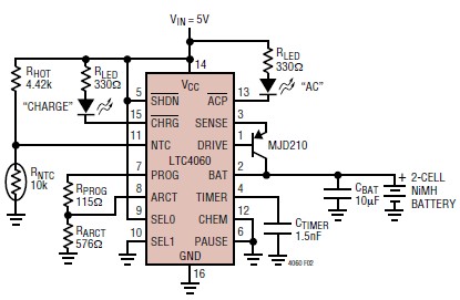
The LTC4060 integrated circuit can be utilized to create a straightforward smart NiMH battery charger electronic project. This charger circuit functions as a complete fast charging system for NiMH or NiCd batteries. It requires only a few external components...
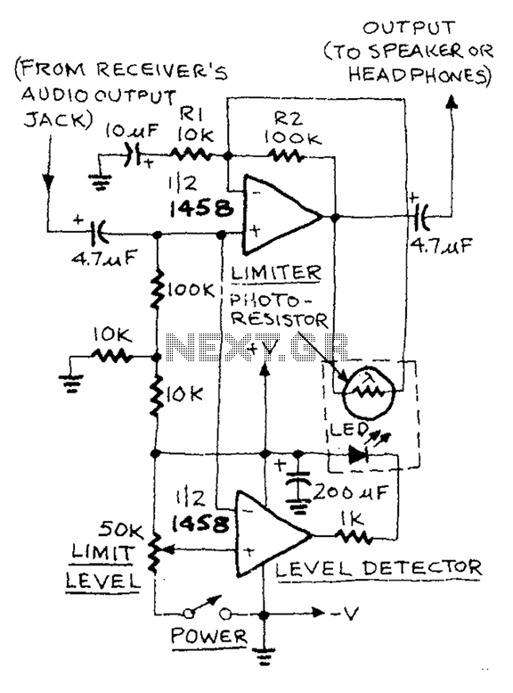
The AUD.LIMITER circuit features a level trim potentiometer that allows for adjustment of the limiting level. When the input signal exceeds the set level of the potentiometer, the output from one half of the operational amplifier, functioning as a...