
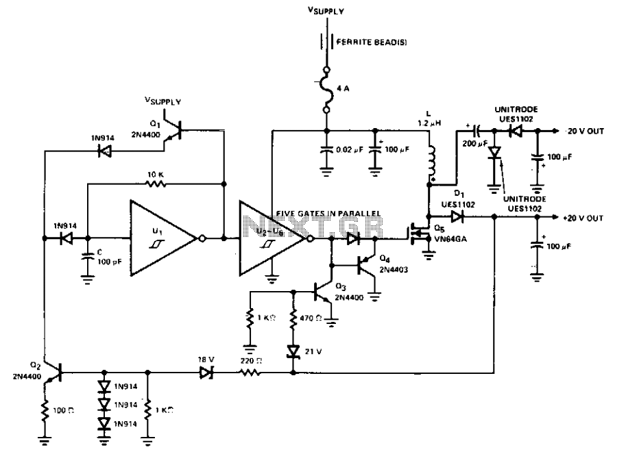
inverter

The inverter circuit described operates efficiently by employing a square wave generation technique, which is essential for converting low-voltage DC to higher-voltage AC. The oscillator, utilizing an integrated circuit (IC), is critical in establishing the desired frequency output, which can be adjusted based on the application requirements. The use of resistors and capacitors in conjunction with the oscillator IC allows for precise control over the frequency and duty cycle, ensuring that the output voltage is stable and suitable for various loads.
The regulation mechanism, which includes a transistor and diodes, plays a pivotal role in maintaining the output voltage within acceptable limits, particularly when dealing with varying load conditions. The incorporation of MOSFETs in the design enhances efficiency, as they provide rapid switching capabilities and lower on-resistance compared to traditional transistors, leading to reduced heat generation and improved overall performance.
The design also addresses the challenges associated with inductive loads, which are common in practical applications. The ability to recirculate idle currents back to the battery minimizes energy loss and enhances the system's efficiency. Furthermore, the thermal protection implemented through the bimetal switch ensures that the inverter operates safely under varying conditions, preventing damage from overheating.
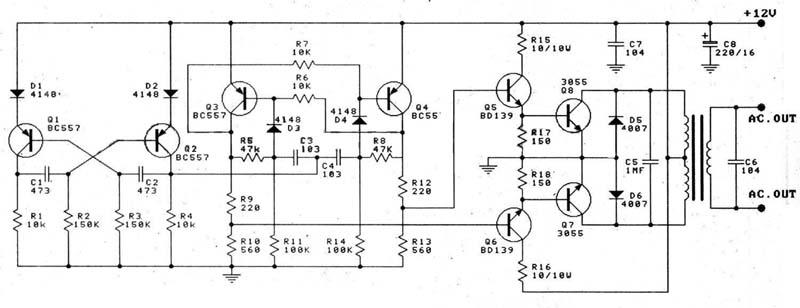
In summary, this inverter design is robust, with well-considered components that work together to provide a reliable source of AC power from a DC source, suitable for a wide range of applications, including those with inductive loads. The careful selection of components, along with the thoughtful arrangement of the circuit, contributes to its effectiveness and efficiency, making it a valuable solution in power conversion applications.The inverter chops the 12 Volt DC Battery voltage into a square wave voltage of 50 cycles per second and duty cycle of 25%, transformed by transformer Tr1 to 230 Volt rms. IC1 forms the oscillator with 100 cycles per second (120 cycles per second for 60 cycles output). Frequency is determined by C1 and the resistors R4 and R5. Resistor R6 determin s the time of the flyback of the oscillator and affects likewise the frequency. In addition, R6 affects the rms of the output voltage, which must be considered if necessary, if the circuit shall be used for other frequencies. 60 cycles per second can be achieved by alignment, higher frequencies require changes in the frequency-determining parts.
For high stability of frequency, special attention must be spent on condenser C1. Ceramic capacitors are not usefull, due to their high sensitivity on temperature. Most foil condensers may keep the frequency quite constant, even against strong temperature variations. IC2 determines the pulse width and thus rms of the output voltage. The regulater consists of transistor T1, which receives its signal from the diodes D4 and D5, taken from the primary tranformer coil.
The regulator adjusts the output voltage by changing the pulse width. It prevents also rising of rms on inductive or capacitive load. The characteristics of regulation can be adapted by changing D4 (important on 24 Volts applications!). Lower voltage level of D4 results in "softer" regulation, i. e. an reduction of the proportional factor. Against earlier versions of the inverter, IC 8 now will be switched directly by the oscillator signal, thus avoiding errors by unexpected oscillations of the PWM-IC 2.
Here the alternate allocation of the impulses for both transistor lines, i. e. for the positive and the negative half wave of the output voltage takes place. The final frequency of 50 cycles per second develops. Flip-flop IC7 stores a switching off instruction of the current limiter for the rest of the half wave. From the gates IC5 (4093-III) and IC6 (4093-IV), the control signal arrives at the complementary MOSFET-driver stage transistors T5/T6 and T7/T8.
T6 and T7 are N-channel-enhancement mosfets and T5 and T8 are the complementary P-channel-enhancement mosfets. These transistors correspond to the well-known CMOS basic circuit (CMOS = Complementary MOS), which represents the basic of the CMOS logic family (CMOS inverters).
Only the resistors R44 to R47 are new in this circuit. They provide current limitation during shifting process and protect in cases of disturbances. The control unit ist suitable for inverters up to 10 kW output power. The driver stage transistors T5 to T8 provide the signals for the power mosfets, which alternately magnetize transformer Tr1. Inductive idle currents, how they are needed e. g. by electric motors, can be returned to the battery, thanks to the integrated antiparallel recirculating diodes of the transistors.
Thus they do not generate unnecessary losses, contrary to early inverters. The most important task in our inverter is done by the mosfet transistors T13 to T28. They are connected in two groups, each of 8 transistors. They generate alternatingly the positive and negative wave of the output voltage. Each transistor line works on ist own transformer coil. After a transistor line is beeing switched off, the magnetic energy stored in the magnetic field of the transformer returns back to the battery by the integrated recirculation diodes of the second transistor line. The idle current of consumers with inductive load takes the same way. In case of strong heating up of the transistors, which should only happen on defects in the equipment, the bimetal thermal switch F2 shuts off the control electronics.
In normal operation, temperature of the heat sink should be as low, that you could touch it by your hands. The source-currents of the mosfet transistors pass over resistor R20 with the very 🔗 External reference
Related Circuits
This PWM control circuit generates control pulses for the DMOS power switch in the flyback circuit. The PWM output produces a pulse width that is proportional to the input control voltage, with the repetition rate governed by an external...
Construct different power conversion circuits using an Arduino microcontroller. The Arduino microcontroller serves as a versatile platform for developing various power conversion circuits. These circuits can include DC-DC converters, AC-DC converters, and other forms of power management systems. The flexibility...
This circuit is a 100W DC inverter based on a transistored multivibrator and serves as a transistor signal amplifier. The inverter converts a 12V DC input voltage to approximately 220V AC. It is recommended to use a 12V car...
This is an astable multivibrator (oscillator) circuit utilizing a CMOS inverter. The circuit employs the CD4007 or MC14007 components. It operates within a frequency range of... The astable multivibrator circuit is designed to generate a continuous square wave output without...
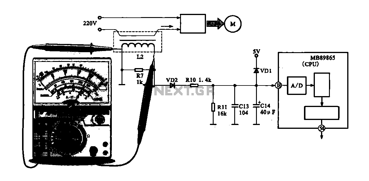
A current-voltage conversion circuit is commonly utilized in current detection applications. An example is the current detection circuit for a ring inverter air conditioner, which primarily serves to monitor the supply current of the compressor motor. Excessive current can...

The plan for the full bridge inverter circuit involves using IRF2807 MOSFETs (75V Vds, 82A Ids) and two IR2110 driver ICs. Previous attempts to create an H-Bridge for a DC motor were unsuccessful. The DC input voltage is 34V,...