
Led display digital Voltmeter

The circuit operates as follows: the voltage to be measured is applied across designated points in the circuit, passing through resistors R3, R4, and capacitor C4 before reaching pins 30 and 31 of the IC, which serve as the input (IN HIGH and IN LOW, respectively). Resistor R1 and capacitor C1 set the frequency of the internal oscillator (clock) at approximately 48 Hz, allowing for about three readings per second. Capacitor C2, connected between pins 33 and 34 of the IC, compensates for errors due to the internal reference voltage and stabilizes the display. Capacitor C3 and resistor R5 form the integration circuit for the input voltage while preventing voltage division, enhancing speed and reliability by reducing error potential. Capacitor C5 ensures the instrument displays zero when no input voltage is present. Resistor R2 and potentiometer P1 are utilized for calibration, ensuring the display reads zero when the input is zero. Resistor R6 regulates the current through the displays, ensuring adequate brightness without damaging them. The IC is capable of driving four common anode LED displays, with the three rightmost displays configured to show digits from 0 to 9, while the leftmost display can only show the number 1 or a negative sign when the voltage is negative.It has been designed as a panel meter and can be used in DC power supplies or anywhere else it is necessary to have an accurate indication of the voltage present. The circuit employs the ADC (Analogue to Digital Converter) I. C. CL7107 made by INTERSIL. This IC i ncorporates in a 40 pin case all the circuitry necessary to convert an analogue signal to digital and can drive a series of four seven segment LED displays directly. The circuits built into the IC are an analogue to digital converter, a comparator, a clock, a decoder and a seven segment LED display driver.
The circuit as it is described here can display any DC voltage in the range of 0-1999 Volts. In order to understand the principle of operation of the circuit it is necessary to explain how the ADC IC works. This IC has the following very important features: An Analogue to Digital Converter, (ADC from now on) is better known as a dual slope converter or integrating converter.
This type of converter is generally preferred over other types as it offers accuracy, simplicity in design and a relative indifference to noise which makes it very reliable. The operation of the circuit is better understood if it is described in tw1o stages. During the first stage and for a given period the input voltage is integrated, and in the output of the integrator at the end of this period, there is a voltage which is directly proportional to the input voltage.
At the end of the preset period the integrator is fed with an internal reference voltage and the output of the circuit is gradually reduced until it reaches the level of the zero reference voltage. This second phase is known as the negative slope period and its duration depends on the output of the integrator in the first period.
As the duration of the first operation is fixed and the length of the second is variable it is possible to compare the tw1o and this way the input voltage is in fact compared to the internal reference voltage and the result is coded and is send to the display. All this sounds quite easy but it is in fact a series of very complex operations which are all made by the ADC IC with the help of a few external components which are used to configure the circuit for the job.
In detail the circuit works as follows. The voltage to be measured is applied across points 1 and 2 of the circuit and through the circuit R3, R4 and C4 is finally applied to pins 30 and 31 of the IC. These are the input of the IC as you can see from its diagram. (IN HIGH & IN LOW respectively). The resistor R1 together with C1 are used to set the frequency of the internal oscillator (clock) which is set at about 48 Hz.
At this clock rate there are about three different readings per second. The capacitor C2 which is connected betw1een pins 33 and 34 of the IC has been selected to compensate for the error caused by the internal reference voltage and also keeps the display steady. The capacitor C3 and the resistor R5 are together the circuit that does the integration of the input voltage and at the same time prevent any division of the input voltage making the circuit faster and more reliable as the possibility of error is greatly reduced.
The capacitor C5 forces the instrument to display zero when there is no voltage at its input. The resistor R2 together with P1 are used to adjust the instrument during set-up so that it displays zero when the input is zero. The resistor R6 controls the current that is allowed to flow through the displays so that there is sufficient brightness with out damaging them.
The IC as we have already mentioned above is capable to drive four common anode LED displays. The three rightmost displays are connected so that they can display all the numbers from 0 to 9 while the first from the left can only display the number 1 and when the voltage is negative the «- « sign. The w 🔗 External reference
Related Circuits

This is a simple design of a single flashlight. This small circuit is within a half hour to build. The circuit operates from 4.5 to 12 V. Of course it is possible other than to drive an LED. More:...
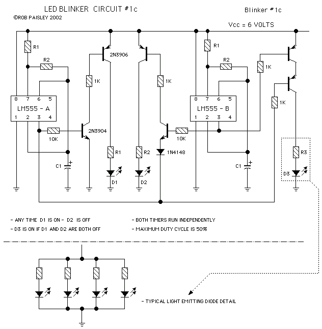
The circuit uses independent timers to flash two light emitting diodes. Any time that light emitting diode D1 is lit, light emitting diode D2 will be switched off. Light emitting diode D3 is on if both D1 and D2...
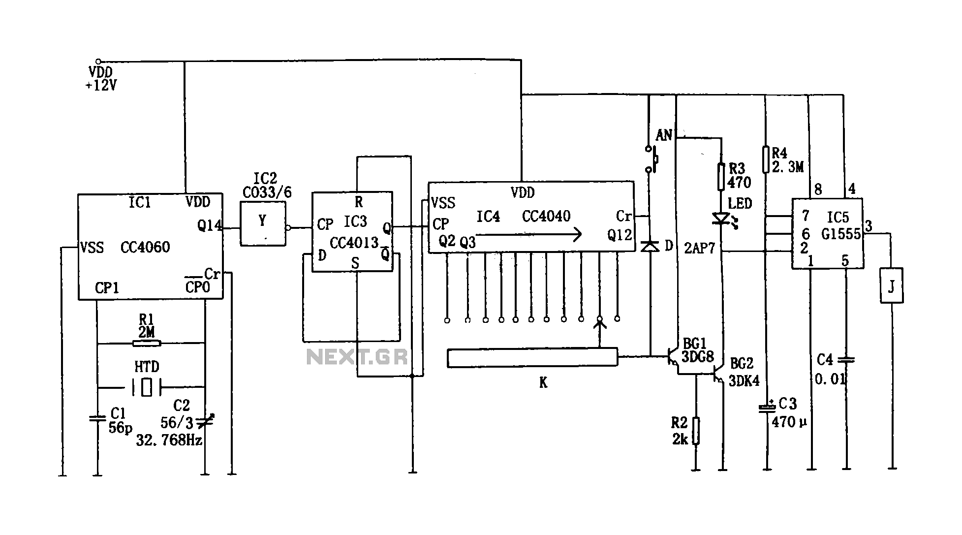
This circuit illustrates a precision digital timing control system. The controller includes a crystal oscillator circuit, a divider, a counting circuit, and monostable flip-flops. The crystal oscillator circuit features a series of 14 binary counters/dividers, a watch crystal operating...
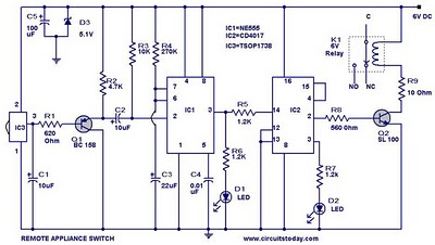
555 Timer TV Remote Controlled Home Appliance Circuit Diagram. Features: 555 timer IC to avoid fast switching. You can only switch the circuit. The 555 timer integrated circuit (IC) is a versatile component widely used in various electronic applications, including...

Analog to Digital Converters - Successive Approximation Type Analog to Digital Converter, working, circuit diagram. The Successive Approximation Register (SAR) Analog to Digital Converter (ADC) is a widely used type of ADC that converts an analog signal into a digital...
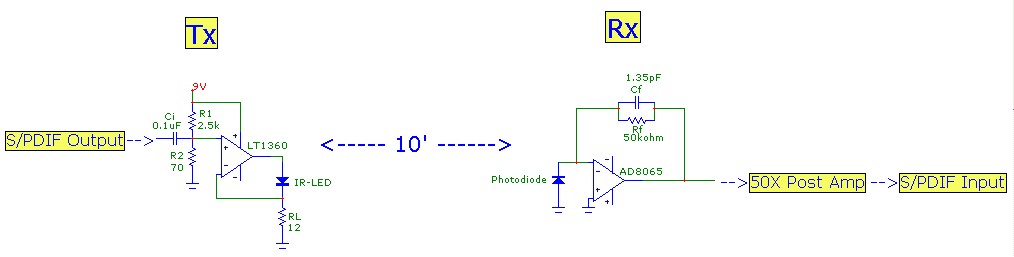
This article aims to illustrate a basic optical LED wireless link for transmitting high-definition (HD) S/PDIF digital audio streams. Circuit designs for both the transmitter (optical modulator) and receiver are provided, utilizing cost-effective op-amp configurations. Specific components are listed,...