
Lights Out circuit

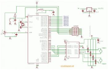
The described circuit utilizes a series of integrated circuits and components to implement a gaming keyboard scanner with additional features for enhanced gameplay. The low-frequency relaxation oscillator, utilizing a 14 Schmitt trigger, provides a stable clock signal at approximately 13 kHz, suitable for the timing requirements of the keyboard scanning process. The phased clock signals generated from the combination of the 4040 counter and 238 de-multiplexer ensure that the system can operate without timing conflicts, allowing for precise sequential event handling.
The initialization of the system through an RC circuit ensures that all logic starts in a known state, critical for reliable operation. The inclusion of a reverse diode serves as a protective measure against potential latch-up conditions caused by unstable power. The random number generation mechanism, based on avalanche breakdown of a PN-junction, introduces variability into the game logic, allowing for unique gameplay experiences.
The keyboard matrix design, consisting of an 8-by-8 array, enables efficient scanning of key presses. The combination of a 4040 counter with de-multiplexer and multiplexer chips allows for systematic checking of each key's state. The use of D-flip-flops for latching button presses ensures that the system captures and retains the state of key presses accurately.
Debouncing is effectively managed through the use of a 688 comparator, which ensures that only valid key presses are registered, enhancing the reliability of user input. The overall architecture of the circuit is designed to facilitate smooth operation, providing a robust platform for interactive gameplay while maintaining a focus on precision and reliability in input handling.The design is based on the previous analysis of calculating the game in a circular shift register. While designing, it occurred to me that small extensions to the design would enable additional game play features, such as replay and manual input. The final design has the following features: The system clock is a low frequency relaxation oscillator
with a `14 Schmitt trigger, running at about 13kHz. The frequency has been chosen to give a scan-cycle time of ~20ms for the keyboard scanner. The clock is combined with the first two stages of a `4040 and a `238 de-multiplexer into a phased clock signal (PHASE0, PHASE1 and PHASE2), which are guaranteed sequential, separated and non-overlapping. A phased clock assures that events can be timed precisely in sequence and prevents glitches from propagating (CPUs use a similar method internally too).
The clock phase generation is coupled with the keyboard scanner (see below). The system is initialized by a common reset circuit setup using a RC charge time coupled to a `14 Schmitt trigger. When the power is turned on, the RC delay holds all important pins at the reset level (CLEAR signal) and thereby initializes the logic to start in a known situation.
The reverse diode (D71) is connected to prevent any latch-up when power is `wonky` (input pins should never be allowed to be at a higher level than the power-supply). The board initialization for each new game is taken from an adjustable random generator. The source of random is a PN-junction in reverse (Q1 base-to-emitter). A high voltage applied at the PN-junction forces it into avalanche breakdown, but when this happens, the applied voltage is reduced through Q2 becoming active (the BE junction of a BC547B starts to break down between 7 and 8 Volts).
The output of Q2 is amplified by Q3 in such way that the Q3 output bias is set at the middle of the `14 Schmitt trigger hysteresis, thereby allowing the Schmitt trigger to alternate at defined levels, but in a random fashion. The bias output of Q3 is adjustable with R105, which alters the position in the hysteresis curve of the `14 Schmitt trigger.
This effectively biases the random towards `0` or `1`, depending the position of R105. A `74 D-flip-flop latches a random value at each PHASE0 so that any reader on the other side will see consistent values. The random data is high frequency and inputs have setup- and hold-times, but the times may vary from chip to chip.
The random data, as input to the game register and the replay register, may not be the same without the synchronization. The keyboard consists of a 8-by-8 matrix of switches (not all are used). The idea is to scan through each row/column combination and see if a key has been pressed. A `4040 counter is used to count from (row, column)=(0, 0) to (7, 7) and each key is sequentially selected using a de-multiplexer + multiplexer combination (`138 and `151 chips).
Whenever a key is pressed, the output BUTTONX will be low for the appropriate coordinate. This is latched in a `74 D-flip-flop to generate a clock-pulse to capture the button press. A pressed button results in the recording of the coordinates in a `273 latch, but no key-press will be asserted if this is the first time detection. When the scanner returns to the same coordinate, some 20ms later, it will then cause the re-recording of the coordinates and push the previous coordinate to a second `273 (an 7-bit wide, 2-bit deep shift-register, as you will).
If the first and second detection of a key-press are at the same coordinates, then the `688 comparator will be active and a key-press will be activated at KEYPRESS. This procedure effectively debounces the key. The de-activation of the KEYPRESS signal is dependent on the detection of "no-button-at-all". For each scan-cycle, it is recorded if any button is pressed (ANYKEY). Only when all buttons are released will the KEYPRESS be released at the end of a scan-cycle an 🔗 External reference
Related Circuits
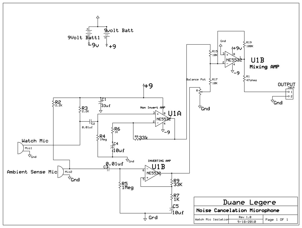
A microphone is designed to listen to a wristwatch while canceling ambient noise in the room. A circuit has been included, which is based on a headphone cancellation circuit. The schematic will be provided shortly. The suggested approach is...
LCD modules have become a popular means of displaying system messages and status in embedded applications. This application note demonstrates how to interface an SST FlashFlex microcontroller to a typical character LCD module. The SST FlashFlex is an industry-standard,...

The circuit illustrated by the PGA204/205 pertains to the shield drive circuit shown in the figure. It is demonstrated through interference theory and practical application that the cable shield, when transmitting weak signals, maintains a certain potential. This configuration...
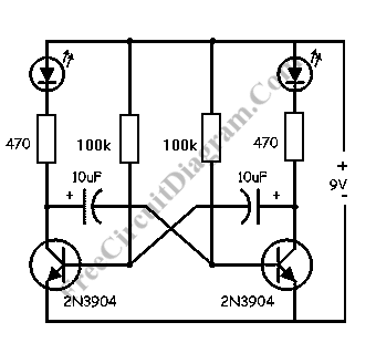
This LED flasher circuit is a classic two-transistor flip-flop. It is a popular circuit often built by beginners in electronic circuit design. The schematic diagram of this well-known LED flasher circuit consists of two transistors, two capacitors, four resistors,...
A high voltage step-up DC power supply using adjustable flyback conversion. The described circuit is a high voltage step-up DC power supply that employs an adjustable flyback converter topology. Flyback converters are widely used in applications requiring electrical isolation and...
The complete electrical circuit diagram of a line follower robot is based on the ATmega16 microcontroller. This robot consists of three primary modules: the sensor module, the microcontroller module, and the DC motor module. A comprehensive tutorial, including circuit...