
Line frequency square-wave generator
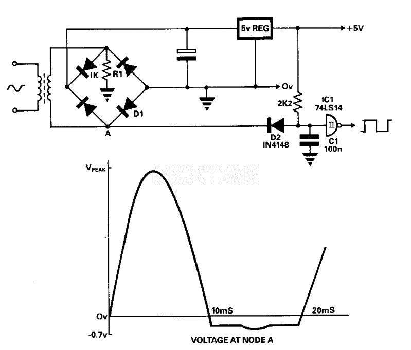
The circuit described utilizes a minimal number of components to produce a reliable square wave output. The fundamental operation relies on the interaction between the diodes in the bridge configuration, which effectively manage the voltage levels at point A. During the positive half-cycle of the input AC signal, diode D1 conducts, allowing current to flow and charging point A. The clamping action of D1, which limits the voltage to approximately -0.7 V, ensures that the output remains within a defined range, preventing damage to the connected components and maintaining signal integrity.
In the negative half-cycle, diode D2 becomes reverse biased when point A rises above +5 V, effectively isolating the output from the input voltage fluctuations. This action stabilizes the voltage at point A, allowing the integrated circuit IC1 to operate within its specified input range. The resistor R1 serves a critical role in loading the transformer secondary, which is essential for maintaining the desired waveform characteristics. By providing a load, R1 helps to prevent waveform distortion that could occur when the diode bridge is not conducting.
Capacitor C1 acts as a transient filter, smoothing out any rapid voltage changes that may occur during switching events. While its inclusion is not mandatory for basic operation, it can enhance the performance of the circuit by reducing noise and providing a cleaner output signal. The careful selection of components and their configuration within the circuit allows for the generation of a stable square wave output suitable for various applications, including signal processing and timing circuits. This design exemplifies the efficiency of simple electronic circuits in achieving complex functionalities with minimal resources.With only three components and a buffer, a line frequency square wave having a 1:1 duty cycle may be derived from the power supply. During the alternate half-cycle, however, A is effectively clamped to - 0.7 V by Dl in the bridge which offsets the forward voltage across D2 giving an input to IC1 of approximately 0 V.
When A rises above + 5 V, D2 is reverse biased and remains at +5 V. Rl is needed to load the transformer secondary maintaining a distortion-free waveform at A during the time the diode bridge is not conducting. Cl although not essential may be required to remove transients. 🔗 External reference
Related Circuits

The Tri-Waveform Generator can be used for a number of different uses. The one that I use it for is a signal generator to test circuits. The frequency range is 20 to 20kHz and can be adjusted by R1....
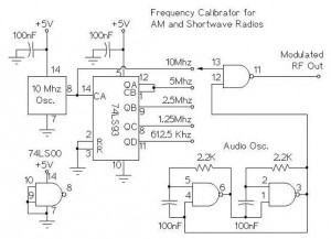
The following circuit illustrates an AM/Shortwave Radio Frequency Calibrator Circuit Diagram. This circuit is based on the 74LS93 IC. Features: The .. The AM/Shortwave Radio Frequency Calibrator Circuit utilizes the 74LS93 integrated circuit, which is a 4-bit binary counter. This...

With this circuit you can mix four separate audio inputs. Each input will accept high or low impedance microphones, phonograph, tape or aux signals. You can adjust the gain of each input by adjusting each respective pot. With the...

This is a phone bug circuit. This wireless telephone line spy circuit can be used to transmit the phone conversation to a nearby FM radio. This circuit must be... The phone bug circuit is designed to intercept and transmit audio...
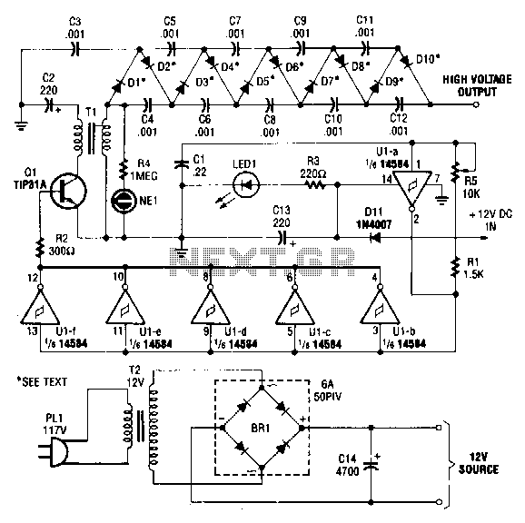
This circuit is powered by a 12-V DC power supply. The input to the circuit is amplified to generate a 10,000-V DC output. The output of the up-converter is subsequently directed into a 10-stage high-voltage multiplier to achieve a...
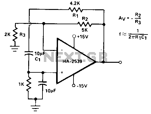
Intended primarily as a building block for a QRI transmitter, this 20-MHz oscillator delivers a clean 6-V peak-to-peak signal into a 100-ohm load. The 20-MHz oscillator functions as a critical component in the design of a QRI transmitter, providing a...