
Low Cost Dimmable Led Ballast Using The Valley Fill Current Shaping Circuit

The BFP640 transistor serves as a critical component in the design of a Low Noise Amplifier for GPS applications operating at 1575 MHz. The primary goal is to enhance the signal received from GPS satellites while maintaining low noise levels to ensure signal integrity. The design specifications are rigorously defined, with a target gain of at least 16 dB to amplify weak signals effectively, while the noise figure threshold of 0.6 dB or lower is crucial to minimize additional noise introduced by the amplifier itself.
The choice of a three-layer FR4 PCB, identified as Infineon Part Number 640-061603 Rev A, provides a robust foundation for the circuit, facilitating effective signal routing and grounding. The use of standard "0402" case-size SMT passive components not only contributes to the compactness of the design but also ensures cost-effectiveness. The layout is optimized for performance, with careful consideration given to the placement of components to minimize parasitic inductance and capacitance.
The LNA's unconditional stability across the frequency range from 5 MHz to 6 GHz is particularly noteworthy, as it ensures reliable operation without the risk of oscillations, which could degrade performance. The choice of components and the PCB design work together to achieve a total area of approximately 35 mm² for the LNA stage, making it suitable for integration into compact GPS receivers.
The amplifier's performance metrics are impressive, achieving a gain of 17 dB and a noise figure of 0.92 dB at the target frequency, with a current consumption of 8.3 mA from a 3.0 V supply. The acknowledgment that the noise figure does not account for PCB losses is critical for understanding the overall performance; the potential reduction of approximately 0.2 dB highlights the importance of accounting for all elements in the signal path.
Furthermore, the input P1dB of -13.1 dBm at 1575.4 MHz indicates the amplifier's ability to handle input power levels effectively, while the input third-order intercept point of +7.7 dBm demonstrates its linearity and capacity to manage intermodulation distortion, which is vital for maintaining signal clarity in multi-signal environments. This comprehensive design approach ensures that the BFP640-based LNA meets the stringent requirements of modern GPS systems.BFP640 used for 1575 MHz Global Positioning Satellite (GPS) Applications BFP640 is investigated for use as an LNA for 1575 MHz GPs Design Goals: Gain = 16 dB min, Noise Figure < 0. 6 dB, Input / Output Return Loss 10 dB or better, current < 10 mA from a 3. 0 Volt power supply, Input P1dB > -14. 8 dBm min Printed Circuit Board used is Infineon Part Number 640-061603 Rev A. Standard FR4 material is used in a three-layer PCB. Please refer to cross-sectional diagram. Low-cost, standard "0402" case-size SMT passive components are used throughout. Please refer to schematic and Bill Of Material. The LNA is unconditionally stable from 5 MHz to 6 GHz. Total PCB area used for the single LNA stage is approximately 35 mm ². Total Parts count, including the BFP640 Transistor is 12. Achieved ‰… 17 dB gain, 0. 92 dB Noise Figure at 1575 MHz from 3. 0 V supply drawing 8. 3 mA. Note noise figure result does NOT "back out" FR4 PCB losses - if the PCB loss at LNA input were extracted, Noise Figure result would be approximately 0. 2 dB lower. Amplifier is unconditionally stable from 5 MHz to 6 GHz. Input P1dB ‰ -13. 1 dBm @ 1575. 4 MHz. Outstanding Input Third Order Intercept of +7. 7 dBm. 🔗 External reference
Related Circuits

The TDA6106Q test circuit, as depicted in the provided figure, operates with a feedback factor of 1/116. The input signal, Vin, is received from the input network consisting of resistors R1, R9 and capacitors C1, C2. The TDA6106Q IC...

In a panic situation during the night when an intruder attempts to break into a house, this alarm system will assist by emitting a loud police siren to deter the intruder. The alarm system is designed to enhance home security...
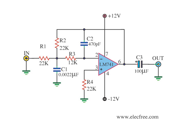
This circuit filters low frequencies below 10 kHz using the highly popular operational amplifier IC uA741. It is convenient for applications that require the conversion of analog signals to digital or vice versa. In digital sound systems, this circuit...
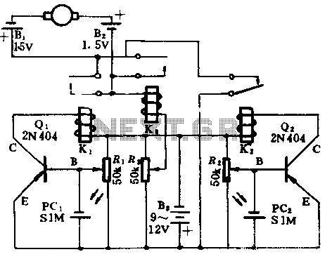
In the absence of light, photocells PC1 and PC2 exhibit high resistance, causing transistors Q1 and Q2 to remain off, which prevents the relay contacts K1 and K2 from closing. The battery B3 is connected through a potentiometer Rs,...
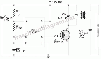
This article presents a driver circuit for a 12V, 5W fluorescent lamp. The circuit utilizes a standard 220V to 10V step-down transformer operated in reverse to achieve a 12V output. The driver circuit for a 12V, 5W fluorescent lamp is...
High pressure alarm with high sensitivity. It detects high-voltage electric energy from 10kV at a distance of 2m or from low-voltage mains (AC 220V) at a distance of 0.3m. The alarm device is simple to manufacture, compact, and user-friendly....