
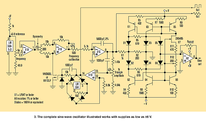
Low-Frequency Crystal Controlled Oscillator

The described circuit serves as a low-frequency sine wave oscillator, designed specifically for testing quartz crystal units within the specified frequency range. The use of bipolar transistors allows for cost-effective implementation without sacrificing performance, while the JFET's role in loop gain control ensures that the oscillator remains stable despite variations in external conditions. The architecture promotes a clean output signal, which is essential for accurate measurements in RF applications.
The modified astable multivibrator configuration, involving transistors Q1 and Q2, is crucial for providing the necessary oscillation and maintaining low distortion levels. The automatic adjustment of the loop gain through Q3 is particularly innovative, allowing the circuit to adapt dynamically to changes in load and environmental conditions. This feature is vital for applications where precise frequency control is required.
The output stage, which includes Q4, not only amplifies the signal but also ensures that the oscillator's characteristics do not degrade due to load variations. The isolation provided by Q5 further protects the output from non-linearities introduced by D1, thus preserving the integrity of the sine wave output. The circuit's design emphasizes reliability and performance, making it a valuable tool for RF engineers engaged in the testing and analysis of low-frequency quartz crystal units.
Overall, this schematic offers a robust solution for the challenges faced in low-frequency testing, combining simplicity, effectiveness, and adaptability in its operation.The RF engineer sometimes has to look for an instrument that will check a low frequency quartz crystal unit reliably and rapidly. This is a difficult piece of equipment to find and the engineer often has to consult an electronic circuits handbook for the schematic of a circuit that will perform the task.
Unfortunately, there aren`t many such circu its in the technical literature currently available, and when found, they don`t always work as expected. A circuit that has been found to work at full satisfaction in the frequency range from 10 kHz to 500 kHz is illustrated in Figure 1.
This is a schematic of a low frequency sine wave oscillator featuring low distortion, wideband operation and crystal control. The circuit, originally developed for laboratory use, employs low cost AF bipolar transistors for the oscillator and amplifier sections and a JFET for loop-gain control.
Operation of the oscillator in the 10 kHz to 500 kHz frequency range has been found to be excellent, while measured distortion is kept under 0. 1 percent. Q1, Q2 and associated circuitry form a modified astable multivibrator in which the loop gain is automatically adjusted to the threshold of oscillation by means of field effect transistor Q3.
Q4 linearly amplifies the signal present at the collector of Q2 and isolates the oscillator section of the circuit from the output. This stage features wideband operation and delivers a clean 2. 5 Volt amplitude sine wave into a resistive load greater than or equal to 20 kohms. The stage comprising Q5 has a voltage gain of 1 and its sole purpose is to isolate the non-linear effects of rectifier D1 from the output.
Transistor Q4 also amplifies the minor changes in amplitude of the oscillator`s waveform due to temperature effects and/or power supply variations, so a magnified version of the perturbance is fedback to rectifier D1 producing a corresponding change in Q3`s gate voltage. This action modifies the FET`s drain-source resistance and hence adjusts the loop gain to a new value slightly above unity, just enough to maintain a constant amplitude in the output.
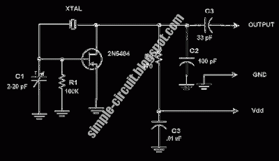
Figure 2 shows optimum values for capacitor C according to the crystal`s resonant frequency. Extra gain is needed from transistors Q1 and Q2 at frequencies below 40 kHz. This is due to the fact that low frequency crystals exhibit large values of series resistance, affecting loop gain (Table 1 compares typical values of series resistance for low frequency units). According to what has been stated, resistor R is made 10 kohms for frequencies under 40 kHz. Above this value, 1 kohm will do. 3) Due to the dynamic action of the JFET the output level is almost insensitive to power supply variations.
The 3. 3 Volt zener diode further enhances this result. 🔗 External reference
Related Circuits
Signals with a known frequency but an unknown phase can be detected using an in-phase signal and a signal that is shifted by 90 degrees, a method commonly utilized in lock-in amplifiers, synchronous detectors, and frequency-response analyzers. The signal...

This design schematic illustrates a Crystal Colpitts oscillator that can be implemented using a transistor and a parallel mode crystal. In this circuit, the crystal functions as an inductance. A large value capacitive divider is utilized between the gate,...
This circuit is a conventional Pierce-type oscillator that utilizes a JFET. It operates with fundamental mode crystals, offering decent performance and reliability when a low noise JFET is employed. The feedback is regulated by the capacitance of C1 from...

The article on the RGB LED fader has been one of the most visited articles on this blog. Since its publication, another microcontroller-based RGB LED project has been designed and built, this time controlling the colors from a computer...
The initial step involves taking notes to indicate which wire connects to each terminal on the 36 tube socket. Remove all wires connected to the 36 tube socket. Next, drill out the rivets that secure the five-pin 36 tube...
Hartley oscillators are inductively coupled, variable frequency oscillators that can be series or shunt fed. They feature a center-tapped inductor and a tuning capacitor, which simplifies the circuit construction. The schematic includes a buffer stage and an amplifier stage...