
Low frequency TTL oscillator

The oscillator circuit described operates based on the principles of feedback and RC timing. The core components include standard inverters, which serve as the primary active elements, along with a resistor and capacitor that establish the timing characteristics. The absence of a minimum operating frequency allows for flexibility in application, making this oscillator suitable for various low-frequency applications.
In terms of component selection, the resistor and capacitor values must be carefully calculated. The resistor value should be chosen to limit the gate current to within safe operating limits specified by the inverter manufacturer. Similarly, the capacitor must be selected to ensure that its leakage current is insignificant compared to the current flowing through the resistor. This is crucial for maintaining stable operation and ensuring that the oscillator functions correctly.
Buffering the output is an essential design consideration. By using a buffer, any variations in the load connected to the oscillator output will not influence the frequency of oscillation. This buffering stage isolates the oscillator from load effects, thereby enhancing the stability and reliability of the circuit.
Furthermore, the circuit's versatility extends to its ability to square up slowly changing logic levels. By incorporating multi-input gates such as NANDs and NORs, the circuit can effectively transform gradual voltage transitions into sharp square wave outputs. This feature is particularly useful in digital applications where clean logic levels are required for reliable operation.
Overall, this oscillator circuit is a simple yet effective design that leverages standard components to achieve reliable oscillation and signal conditioning, making it suitable for various electronic applications.This oscillator uses standard inverters, one resistor and one capacitor, and has no minimum operating frequency. R and C must be chosen such that currents into the gates are below recommended operating limits and that leakage current into the gates and into C are small in comparison with the current in R also the output should be buffered (13) to prevent variations in load affecting frequency.
This circuit may also be used to square up slowly changing logic levels by use.of multi input gates (NANDS, NORS Etc).
Related Circuits
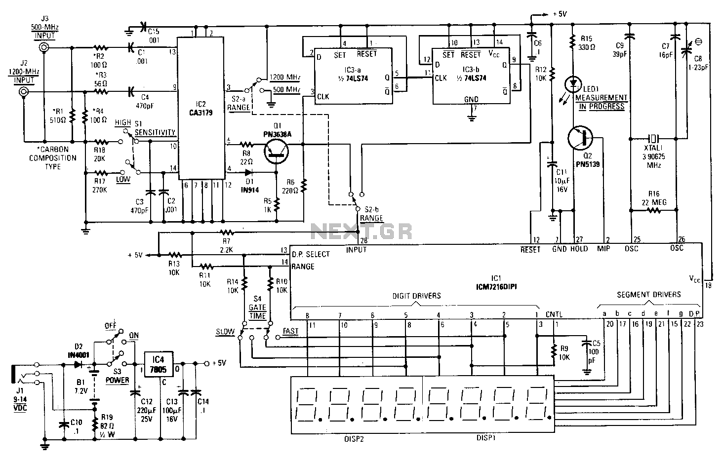
The output of the CA3179 is fed through the D1Q1 circuit. These components serve to boost the 1V output of the CA3179 to a standard TTL level. Depending on the position of range switch S2b, the signal is passed...
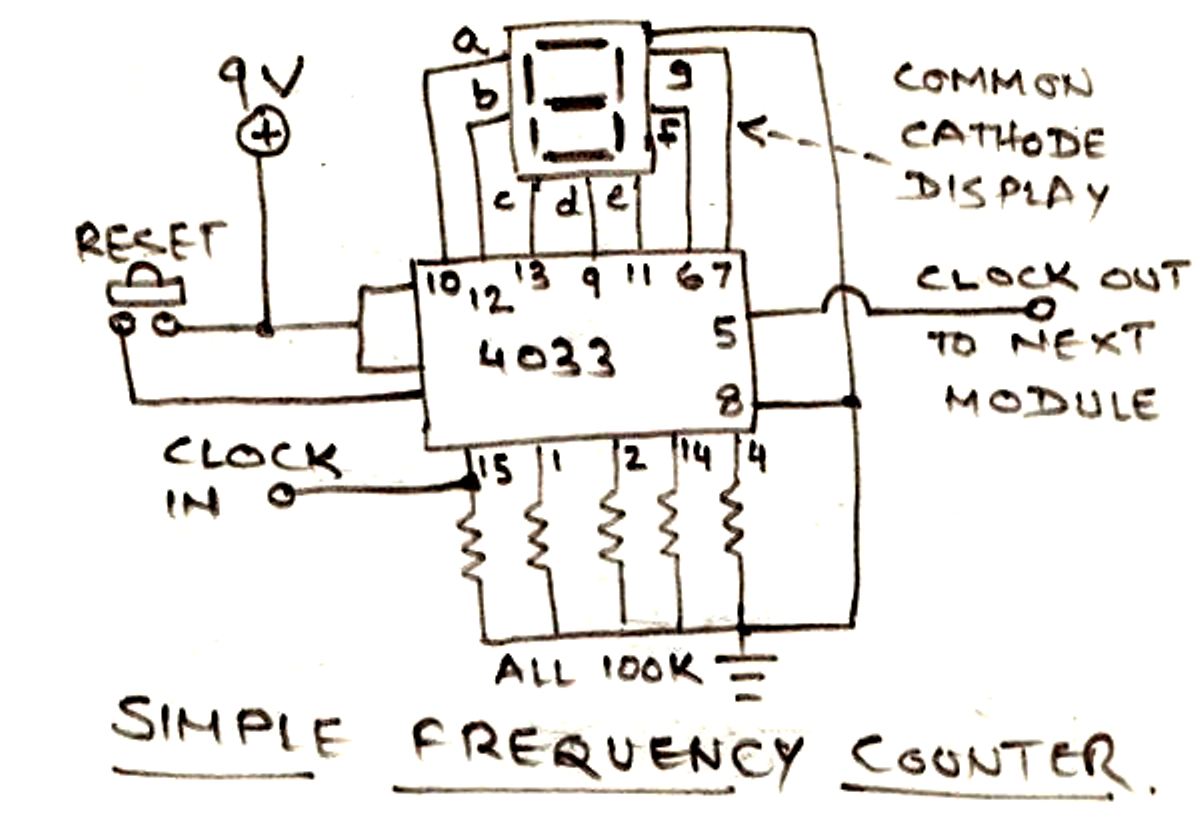
The circuit illustrated below is designed for measuring frequency in Hertz (Hz). It is straightforward to construct, utilizing a single IC 4033 and a common cathode display as the main components. For measuring higher frequencies, typically in the range...
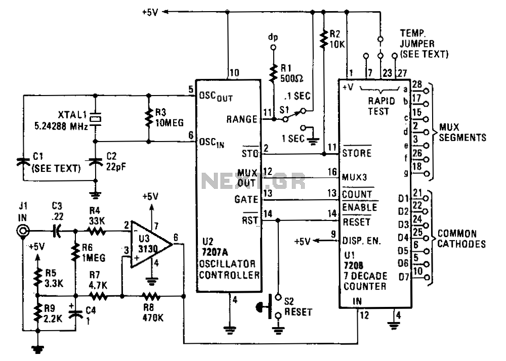
The circuit comprises an ICM7208 seven-decade counter (U1), an ICM7207A oscillator controller (U2), and a CA3130 biFET operational amplifier (U3). The ICM7208 (U1) counts input signals, decodes them into a 7-segment format, and outputs signals to drive a 7-digit...
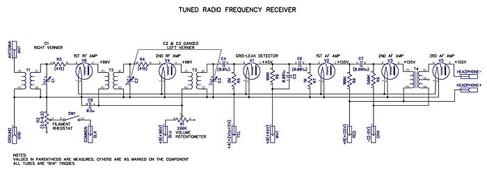
Tuned radio frequency receiver. A radio receiver consisting of several amplifier stages that... A tuned radio frequency (TRF) receiver is a type of radio receiver that utilizes multiple amplification stages to enhance the reception of radio frequency signals. The design...

This circuit represents a waveform generator, which is highly beneficial for electronic experiments and design. It primarily generates sine wave oscillations, but the circuit can be modified to produce triangle or square wave functions. The circuit is based on...

Applying the filtered and rectified AC input to a high-input-voltage linear regulator is the simplest way to produce a low current level from an AC source. The process of converting an AC source to a low current level using a...