
Low-Offset Simple Video Buffer Circuit

The described circuit functions as a video buffer designed to interface with video signals while maintaining signal integrity. It is capable of driving a standard 75-ohm load, which is commonly used in video transmission systems. The output voltage level of 1.5 V peak-to-peak is suitable for compatibility with typical video equipment.
The bandwidth specification of greater than 20 MHz indicates that the circuit can handle high-frequency video signals, making it suitable for applications involving video processing or transmission. The low DC offset of less than 0.05 V ensures minimal distortion in the output signal, which is critical for maintaining image quality in video applications. This small offset arises from the characteristics of the bipolar junction transistors (BJTs) Q1 and Q2, where their base-emitter voltage (VBE) variations contribute to the overall performance of the circuit.
To ensure optimal performance, it is crucial that the power supply lines are well bypassed. This means that decoupling capacitors should be placed close to the power pins of the circuit to filter out high-frequency noise and stabilize the supply voltage. A supply voltage of 5 V or more is recommended to provide adequate headroom for the circuit's operation while ensuring reliable performance across the specified bandwidth.
In summary, this video buffer circuit is well-suited for applications requiring robust signal handling and minimal distortion, making it a valuable component in video signal processing and transmission systems. Proper power supply management will further enhance its performance and reliability. This circuit has proved to be an effective video buffer and will easily drive a 75- load to 1.5-V p-p output. BW is better than 20 MHz and there is less than 0.05-V dc offset, which is the difference in VBE of Ql and Q2.
The supply lines should be well bypassed, 5 V or more.
Related Circuits

This circuit generates the power required to operate a bipolar stepper motor. It allows for adjustments in both the rotation speed and direction of the motor. The design includes two integrator circuits (A1, A3) and an amplifier (A2) connected...
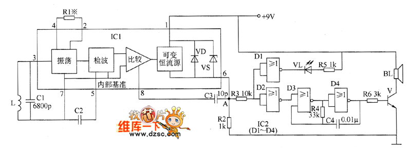
The metal detector circuit comprises an oscillator and a sound-light alarm circuit. The oscillator circuit includes an inductor (L), a capacitor (C1), a sensor switch integrated circuit (IC1) that integrates the oscillator, detector, comparator circuit, and peripheral components. The...
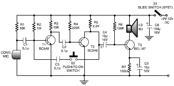
This is a low-cost and simple intercom circuit design that utilizes three transistors. Even a novice can assemble it on a piece of veroboard without difficulty. The intercom circuit is designed to facilitate two-way audio communication between two locations. The...

The circuit consists of four light-controlled electronic switches, timing circuits, voice circuits, audio circuits, and other components. It is designed to celebrate birthdays or similar occasions, with features such as birthday candles that can be lit or extinguished. The...
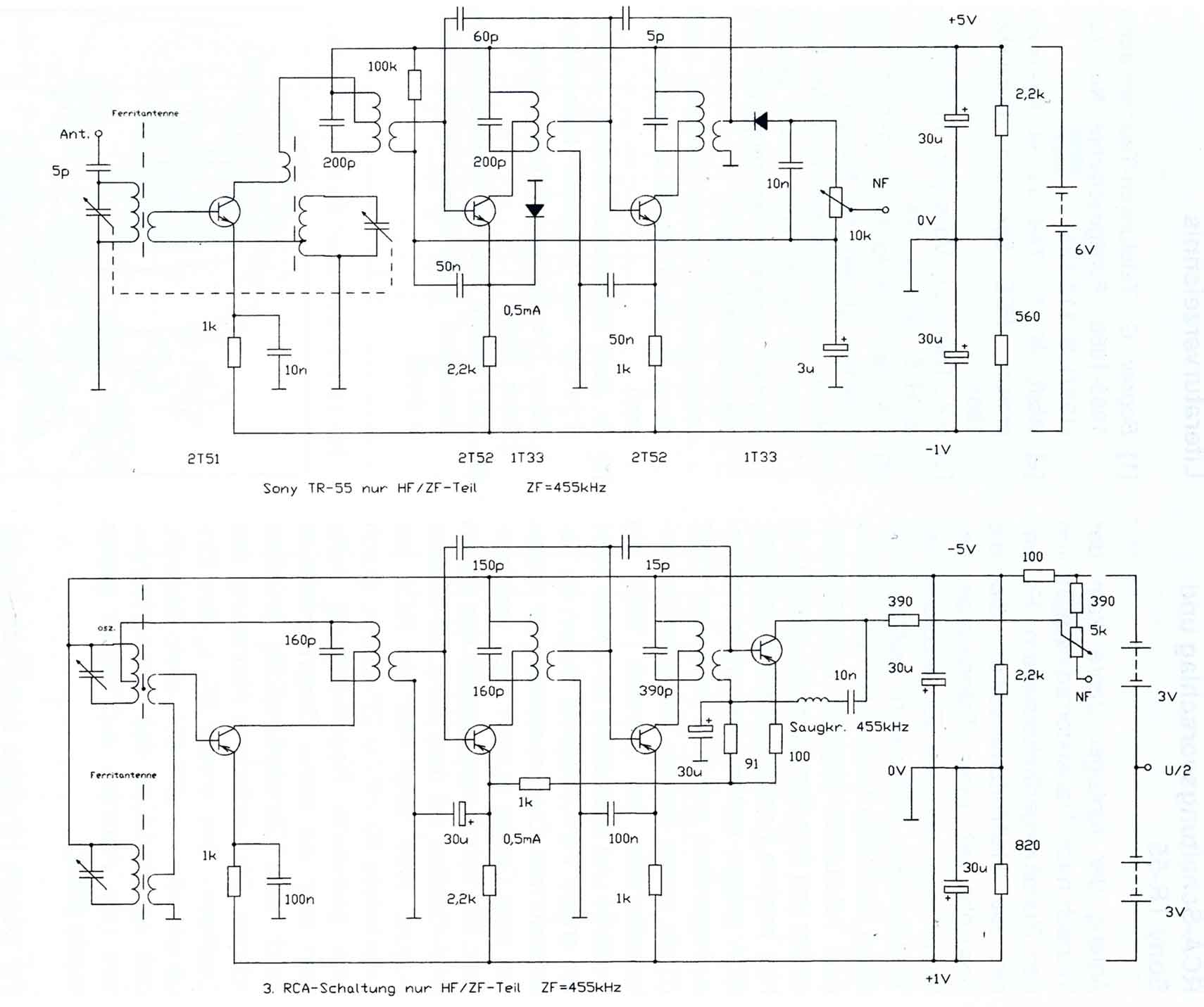
The circuitry of the Regency exhibits several unique characteristics. Notable features include the self-oscillating mixer stage, the base bias voltage of the second IF stage derived from the AF power stage, an unusual IF frequency of 262 kHz, and...
The use of a quarter-wave parallel-wire line as a tuning unit has been discussed in the chapter on Short Lines, where it was pointed out that these circuits have comparatively high Q even at higher frequencies. Their great length...