
low power inverter using cd4047

The square wave inverter circuit designed with the CD4047 IC operates efficiently for low power applications, making it suitable for various basic power supply needs. The astable configuration of the CD4047 allows for continuous oscillation, which is essential for generating the square wave output required for inverter operation. The choice of a variable resistor (RV1) enables users to fine-tune the frequency output, ensuring compatibility with standard AC loads that require a 50 Hz input.
The pre-amplification stage using TIP122 transistors is critical for boosting the current levels to drive the 2N3055 power transistors effectively. The configuration of these transistors in parallel not only increases the current handling capacity but also enhances the reliability of the inverter under load conditions. The use of a Zener diode ensures that the voltage supply to the CD4047 remains stable, which is crucial for maintaining consistent operation and performance.
In terms of output waveform, the inverter produces a square wave, which is adequate for resistive loads but may not be ideal for sensitive electronic devices that require a pure sine wave. However, this design serves well in applications where simplicity, cost-effectiveness, and ease of construction are prioritized. Overall, this low-power square wave inverter design using the CD4047 IC demonstrates a practical approach to meeting basic inverter requirements in various applications.For basic requirements we can use Square Wave Inverters which is very simple, low cost and easy to make. But for driving inductive loads pure sine wave inverters are preferred. Here we are dealing with a Simple Low Power Square Wave Inverter using CD4047. It doesn`t include battery charging circuit which is present in most of the inverters. It can be used to power up to 100w. CD4047 is a low power IC capable of operating in either in astable or monostable mode. Here it is wired in astable mode. It works by charging a capacitor (C2) through aG‚resistorG‚(RV1) as in every astable multivibrators. Variable resistor (RV1) is provided for adjusting the output frequency to exact 50Hz. The time period of the oscillation is given by the relation T = 4. 40*R*C. For detailed working of the IC, please refer its datasheet. CD4047 has two outputs (pins 10 and 11) which areG‚complementaryG‚to each other. These square wave pulses are pre amplified by TIP122 transistors. This amplified current is used to switch 2N3055 transistors to drive the inverter transformer. Two 2N3055 transistors are connected in parallel to increase the current driving capabilities. The Zener Diode ZD1 and capacitor C2 is used to provide constant 9V for the IC. When the output at pin 10 is low, pin 11 will be high Q1, Q3, Q4 turns on, current flows through the upper winding of the transformer and we will get positive half cycle output. When the output at pin 10 is high, pin 11 will be low Q2, Q5, Q6 turns on, current flows through the lower winding of the transformer and we will get negative half cycle output.
🔗 External reference
Related Circuits
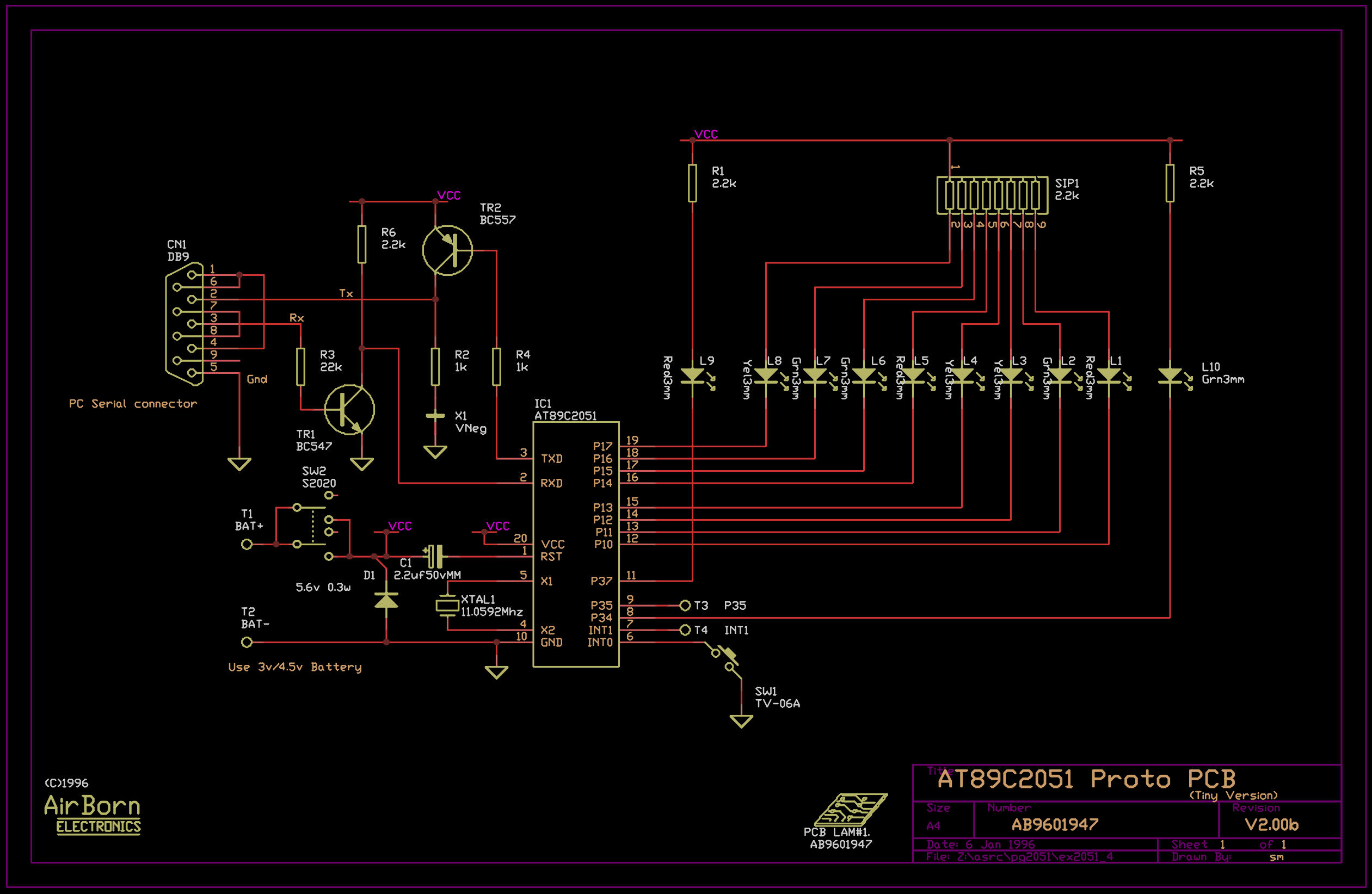
The example program included with the PG2051 evaluation kit is a basic serial to parallel converter written in 8051 assembler. This is probably a good example of the uses to which an AT89C2051 can be put - it would...
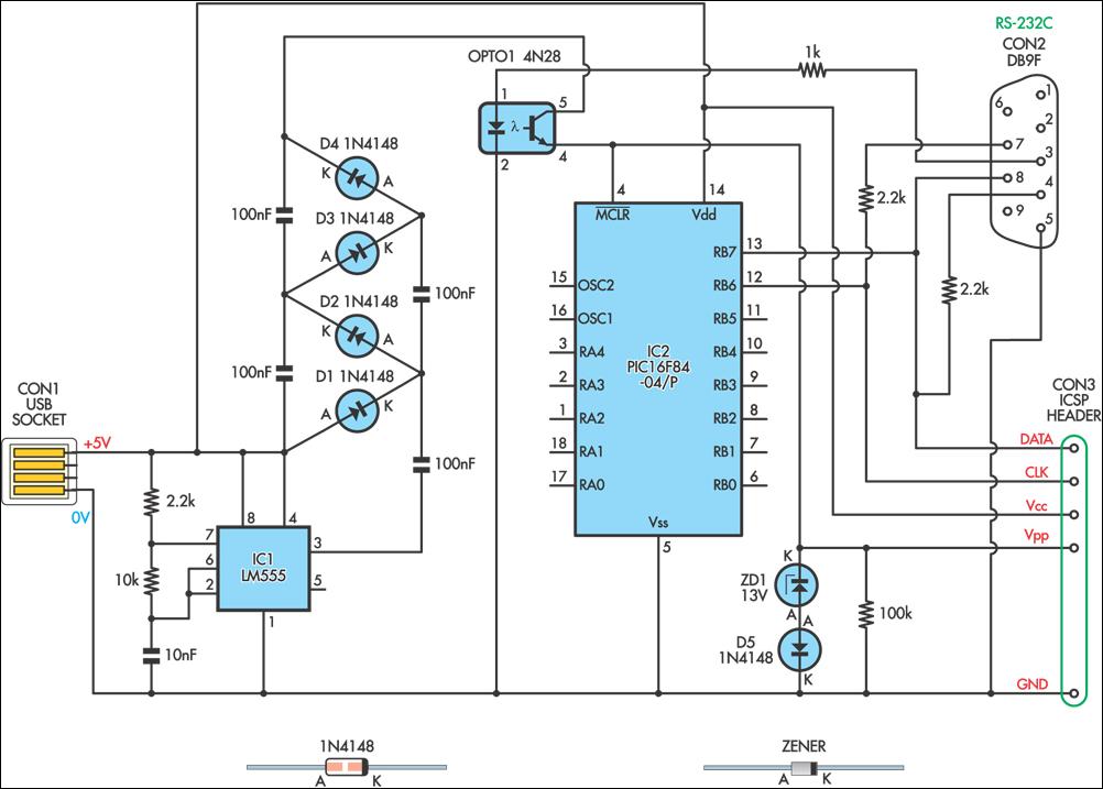
This simple circuit can be used to program the PIC16F84 and similar "flash memory" type parts. It utilizes a 555 timer IC to generate the programming voltage from a +5V rail, allowing the circuit to be powered from a...

C1 is a 1000 microfarad aluminum electrolytic capacitor. For loads less than 100mA, a 220 microfarad capacitor can be substituted. The voltage rating should be 2.5 times the output voltage. C1 serves as a critical component in various electronic circuits,...
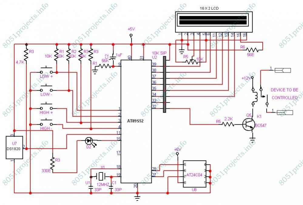
This project is designed to monitor and control temperature. The system utilizes the DS1820 temperature sensor to measure the temperature, which is then displayed on an LCD. It features two preset levels: a low preset and a high preset....

The AD7740 is the smallest and most affordable 12-bit Voltage-to-Frequency Converter (VFC) available. As a synchronous converter, its output frequency is tied to a fixed master clock frequency, which enhances temperature stability compared to asynchronous VFCs. With a 1...
As readers may know, there are several power amplifier projects, including two that utilize integrated circuit (IC) power amplifiers, commonly referred to as power op-amps. Both of these projects have gained popularity, and this new project is not intended...