
Mains clearance in a TRIAC driver

The TRIAC driver board is designed to manage high-voltage AC loads, making it essential to adhere to safety and clearance standards outlined in IPC-2221. The use of a 2-layer FR4 PCB is standard in such applications, providing adequate insulation and mechanical stability. The overlapping or tapering of tracks is a critical consideration in high-voltage designs, as it can affect the dielectric breakdown and overall reliability of the circuit.
The separation between high-voltage and low-voltage sections must exceed the minimum clearance requirements, which ensures safety against accidental shorts and arcing. The zero-crossing detector circuit, while simple, plays a crucial role in synchronizing the TRIAC operation with the AC waveform, enabling effective PWM control. The choice of components, specifically the power rating of resistors and capacitors, must be carefully considered to handle the expected voltage and current levels.
In terms of layout, the positioning of the heatsink is vital for thermal management, especially in high-current applications. The decision to avoid a snubber circuit is justified if the load remains purely resistive; however, it is essential to monitor the system for any potential inductive effects that could arise from wiring or component placement.
The discussion regarding solder thickness and track width is pertinent, as increased trace thickness can enhance current-carrying capacity, but it must be balanced with PCB design rules to prevent excessive heat generation and ensure reliable operation. The phase shift due to capacitive elements in the circuit can significantly influence the timing of the TRIAC's operation and should be taken into account during the design phase.
Overall, the design of the TRIAC driver board should focus on maintaining safety, reliability, and efficiency through careful consideration of component selection, layout, and adherence to established electrical standards.A TRIAC driver board for use with my reflow toaster oven project, which means mains voltages. IPC-2221 says that U. S. mains voltages require 0. 4mm clearance if coated with solder mask. A few questions: Can I run overlapping tracks on both sides of the board I don`t know how thick the PCB is but it`s a standard, 2-layer FR4 PCB. Since the 200 mil "tracks" (fills, actually) running from the screw terminal to the TRIAC are sort of, erm, wide, they have to either overlap or taper at the ends. How much clearance do I need between the high-voltage section and the low-voltage section I`ve kept them at least as far apart as the opto-isolators are wide but I`m curious what the standards say. I haven`t finished checking clearances yet but any comments about the circuit or the PCB are welcome.
The top of the schematic is the TRIAC driver of course, and the bottom is a zero-crossing detector. I`m especially curious whether I really need two capacitors and two resistors for the detector, I got that from a Fairchild app note but there weren`t any voltage or safety ratings in the example so I had to assume the worst. For the zero-cross detector you can use only a single resistor instead of two caps and two 1K resistors but you will need a high power rating resistor (10K/5W for 120V AC mains or 22K/7W for 240V AC).
Thanks for the advice. The reason I`m not using a zero-crossing opto-TRIAC is that I want to PWM the output - the detector is for keeping the pulses in sync with the AC waveform while still allowing me to delay them to get the varying levels of power I want. I also opted not to use a snubber since the load is always purely resistive, and the connector is where it is because that big pink thing is a rather large heatsink :-) That said, I do intend to move it to the right-hand side in an attempt to squeeze this onto a smaller PCB.
Why do you recommend narrower tracks and solder coating I thought the conductance of solder was relatively bad, but I guess that would matter less since it would be much thicker than the copper. Another problem is that the tracks would no longer be soldermask-coated so I would need the full 3. 2mm clearance required by IPC-2221. Thanks for the advice. The reason I`m not using a zero-crossing opto-TRIAC is that I want to PWM the output - the detector is for keeping the pulses in sync with the AC waveform while still allowing me to delay them to get the varying levels of power I want.
I also opted not to use a snubber since the load is always purely resistive, and the connector is where it is because that big pink thing is a rather large heatsink :-) That said, I do intend to move it to the right-hand side in an attempt to squeeze this onto a smaller PCB. Why do you recommend narrower tracks and solder coating I thought the conductance of solder was relatively bad, but I guess that would matter less since it would be much thicker than the copper.
I hope you`re aware you need to account for the phase shift generated by the capacitors you`ve used to limit the current to the LEDs. In a purely capacitive circuit (which nearly to what you have) the current leads the voltage by 90o so one LED will turn on and the other turn off as the mains voltage passes its peak, which will briefly turn 0Q1 off for a few hundred µs.
I don`t see what`s the problem in using solder to make the traces thicker. We are not talking about 1km of PCB trace; just a few centimeters. If it works for car amplifiers where the currents are around 40-60A (and with longer PCB traces) then I really don`t see a problem with this application. You don`t have to leave entire trace exposed - just leave the middle of the trace exposed. 120V. I was referring to mains-to-mains clearance, not low-voltage clearance, according to IPC-2221 rules at 170V peak-to-peak.
The low-voltage side is still off in its own little corner no matter what I do to the high-voltage tracks. It`s i 🔗 External reference
Related Circuits

A relay is an effective solution for switching a mains voltage circuit, particularly in applications where long switching times and high currents are present. However, a... A relay is an electromechanical switch that uses an electromagnetic coil to control the...

This lighting solution offers over 90% energy savings compared to incandescent or halogen bulbs, with a lifespan exceeding 50,000 hours. It operates without flickering, making it suitable for human eyes, and produces no RF interference or UV radiation. The...

Downloading and CD-burning programs often offer the option to automatically shut down the PC upon completion of their tasks. However, this energy-saving feature is ineffective if all peripheral equipment remains connected to the mains and continues to consume power...

A simple white LED driver schematic can be created using the EL7513 constant current boost regulator, which is specifically designed for driving white LEDs. This driver can manage 4 LEDs in series or up to 12 LEDs in a...

The BQ2000 is a programmable, monolithic integrated circuit designed for fast-charge management of nickel cadmium (NiCd), nickel metal-hydride (NiMH), or lithium-ion (Li-Ion) batteries in single or multi-chemistry applications. The BQ2000 detects the battery chemistry and employs optimal charging and...
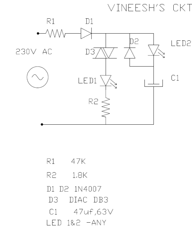
The following mains-operated LED flasher circuit, which is essentially an astable multivibrator circuit, utilizes a diac and resistor arrangement to achieve an interesting wig-wag flashing effect with two LEDs. The circuit was shared by Mr. Vineesh, a dedicated follower...