
MAX2664/MAX2665 VHF UHF Low Noise Amplifiers Circuit

The circuit utilizes the MAX2664 and MAX2665 as the core components for amplification in VHF/UHF applications. The MAX2664 is optimized for UHF frequencies, providing a gain of around 15 dB, which is essential for enhancing signal strength in various communication devices. The MAX2665, on the other hand, is tailored for VHF applications, ensuring that signals within the 75 MHz to 230 MHz range are amplified efficiently.
The design incorporates a single power supply, simplifying the overall circuit layout and reducing component count. The power supply requirements of 2.4 to 3.5 volts ensure compatibility with a broad range of battery-operated devices. The low current consumption of 3.3 mA allows for extended battery life, which is a critical factor in portable applications.
The integrated bypass switch in both ICs serves a dual purpose: it allows for the amplification of weak signals while providing a means to bypass the amplifier during high-signal conditions, thereby preventing distortion and ensuring optimal performance. The zero-power bypass mode is particularly advantageous in scenarios where high signal levels are encountered, allowing the device to conserve power when amplification is not necessary.
Overall, this circuit design represents an efficient solution for low-noise amplification in VHF/UHF applications, making it ideal for modern electronic devices that require reliable performance in compact form factors. The minimal external component requirement further enhances its suitability for integration into various consumer electronics.Here`s a design circuit for very simple low cost and ultra compact VHF UHF Low-Noise amplifiers circuit can be designed using the MAX2664 and MAX2665 ultra-compact LNAs for VHF/UHF applications. These devices incorporate a broadband LNA with an integrated bypass switch. The MAX2664 covers the UHF frequency range from 470MHz to 860MHz, and the MAX2 665 covers the VHF frequency range from 75MHz to 230MHz. Each device has a zero-power bypass mode for improved high-signal-level handling conditions. This is the figure of the circuit; As you can see in the presented circuit diagram, this RF project requires very few external components. Both ICs has a high gain around 15dB and require a single power supply, that can provide an output voltage between 2.
4 to 3. 5 volts. VHF UHF Low-Noise amplifiers has a very low current consumption of 3. 3 mA and can be used in applications like: Smart phones/Handsets, MP3 Players, Home Audio/Video and other portable navigation devices. 🔗 External reference
Related Circuits
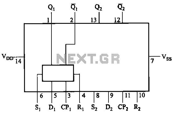
The CD4013 is a dual D flip-flop that operates on the rising edge of the clock signal. Its internal block diagram and pin configuration are provided. This device is part of the standard model C043 and the GB model...

When the asterisk (*) is pressed on the touch-tone phone, a DTMF decoder, referred to as TCI, manages the on-hold logic. Audio from the FM receiver IC4 is transmitted over the telephone line when a hold condition is active....
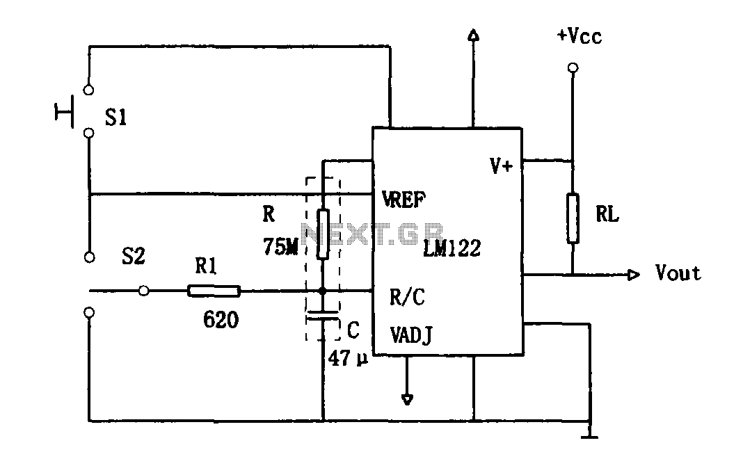
As illustrated in Figure 1, the circuit utilizes an LM122 timer. The circuit's start, reset, and stop functions are managed through switching operations. Switch S1 initiates the timing sequence when the timer is activated; thereafter, this switch has no...
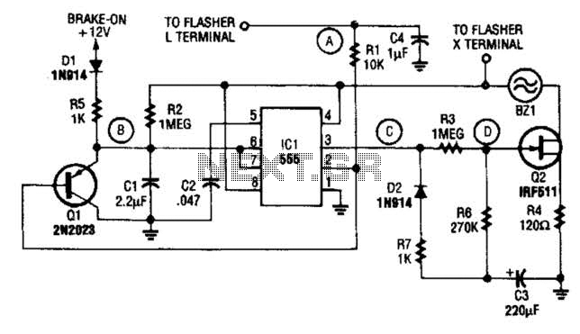
The STS schematic illustrates a circuit designed to alert a driver when the turn signal has been active for more than 15 seconds. The voltage at the gate of transistor Q2 increases in response to the charge accumulated on...
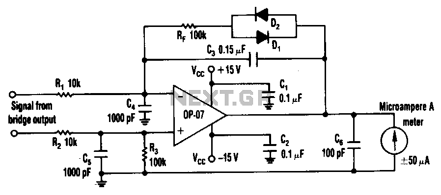
The circuit can utilize any general-purpose, low-offset, low-drift operational amplifier (op amp), such as the OP-07. The differential signal from the bridge feeds into an amplifier that drives a standard, rugged ±50 µA meter. However, near the null point,...
Designed to power a low-frequency subwoofer speaker system, the amplifier can deliver up to 100 W into an 8-ohm load. The OPA541BM operational amplifier, produced by Burr-Brown Corporation, necessitates heatsinking for optimal performance. Additionally, the design incorporates a damping...