
CD4013 circuit

The CD4013 dual D flip-flop is a versatile digital memory circuit used for storing binary information. Each flip-flop has two inputs, D (data) and CLK (clock), and two outputs, Q and Q' (complement of Q). The flip-flop captures the value present at the D input on the rising edge of the CLK signal, transferring this value to the Q output. The Q' output always reflects the inverse of the Q output.
The internal structure of the CD4013 consists of multiple stages of logic gates configured to form the flip-flop functionality. The device operates with a supply voltage range of 3V to 15V, making it suitable for various applications in both low and high voltage environments. The propagation delay between the clock input and the output state change is typically around 50 nanoseconds at a supply voltage of 5V, which makes it suitable for moderate-speed applications.
Pin configuration is critical for proper integration into circuits. The CD4013 has 14 pins, with the primary pins being:
- Pins 1 and 2: D input and CLK input for the first flip-flop.
- Pins 3 and 4: Q output and Q' output for the first flip-flop.
- Pins 5 and 6: D input and CLK input for the second flip-flop.
- Pins 7 and 8: Q output and Q' output for the second flip-flop.
- Pins 11, 12, 13, and 14 are used for power supply and ground connections.
The CD4013 is widely used in digital circuits for applications such as data storage, state machines, and frequency division. Its ability to interface with various logic families enhances its applicability in diverse electronic designs. The interchangeable models (TC4013, MC14013, etc.) offer flexibility in sourcing components while maintaining compatibility with the original design specifications.CD4013 dual D flip-flop on the rising edge. Its internal block diagram and pins are shown. Ministry of standard model C043, GB model CC4013, substitutable or interchangeable models TC4013, MC14013, C073, SG822 and the like.
Related Circuits
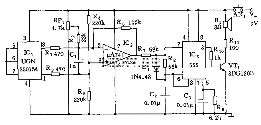
The circuit consists of a 555 timer and associated components designed for voltage-to-frequency conversion. It is utilized for determining the orientation of Earth's magnetic field using a Hall-effect sensor, specifically the UGN-3501M. This sensor incorporates a Hall element and...
The two drawings utilize the LM324 operational amplifier to create a low-voltage comparator. Resistor R1 is part of a voltage divider circuit, while operational amplifier A1 is configured to a reference voltage level U1. Resistor R2 forms another voltage...
The Quick and Easy Wireless circuit is not overly complex, but it requires careful verification of connections before initial operation. Key components in the circuit include the 7805 voltage regulator, the 18F452 microcontroller, an RC Receiver, and an RC...
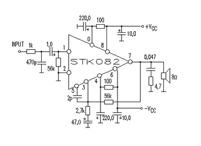
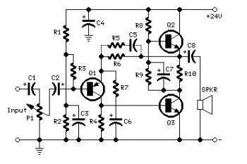
This amplifier circuit is suitable for home power audio devices. The STK082 amplifier specifications suggest that it can operate with supply voltages of up to ±43V. However, it is advisable to use no more than ±25V for 8-ohm loads,...
The total electric current drawn by the circuit should be measured by connecting the probes of a multimeter across the positive output of the power supply and the positive rail input of the amplifier. The expected current value is...
This 2-meter 144 MHz fox hunt transmitter is utilized in amateur competitions where participants seek to locate a concealed transmitter using primarily homebrewed receivers. The 144 MHz fox hunt transmitter is designed for use in amateur radio competitions, commonly referred...