
Metronome Circuit

The circuit design integrates two CA741 op-amps, each serving distinct roles in sound generation. The first op-amp operates as an astable multivibrator, generating square wave pulses. The timing of these pulses is determined by the resistor R2, the variable resistor VR1, and capacitor C1, which together define the frequency of oscillation. The output from the astable configuration is then filtered through capacitor C2, which blocks DC components while allowing the AC signal to pass, ensuring that only the timing pulses are forwarded to the second op-amp.
The second op-amp is configured as an integrator, which modifies the incoming square wave pulses into a ramp signal. This ramp signal undergoes further distortion to create the ringing effect, which is critical for achieving the desired sound quality. The zener diode ZD1 plays a crucial role by providing a reference voltage, allowing the transistor Q1 to switch on during positive transitions of the output pulse. This switching action enhances the overall dynamic response of the circuit.
Resistor R8 is strategically placed at the input of the integrator to provide a low impedance path, which helps shape the output sound into a "tock" effect. The interaction between R8 and the integrator's feedback components, R7, R9, along with capacitors C3 and C4, allows for fine-tuning of the sound characteristics. Adjusting these components can significantly alter the timbre and duration of the generated sound, enabling the user to customize the output to meet specific auditory preferences.
In summary, this circuit effectively combines astable and integrative configurations of op-amps to produce a distinctive sound effect characterized by its rhythmic "tick" and "tock" qualities. The design allows for flexibility in sound modulation, making it suitable for various audio applications.This circuit uses a couple of Op-amps to produce an interesting sound effect. The left hand CA741 is wired as a standard astable and produces the timing pulses, controlled by C1, R2 and VR1. The output is fed via C2 to the second op-amp and is also direct coupled via the zener ZD1 to Q1. The right hand CA741 is configured as an integrator, its pur pose being to distort the output pulse from the first op-amp. This produces a ringing effect on the output pulse and gives the circuit a characteristic "tick" sound. A sound sample recorded under Audacity on PCLinuxOS is shown below. The emphasized ringing can be seen in the enlarged view above. The output pulse at the first op-amp will cause the zener and Q1 to conduct on every positive transition.
The 1k resistor R8 then acts as a low impedance shunt at the input of the integrator and produces a characteristic "tock" effect. R8, R7, R9, C3 and C4 may all be adjusted to tailor the sound effect. 🔗 External reference
Related Circuits
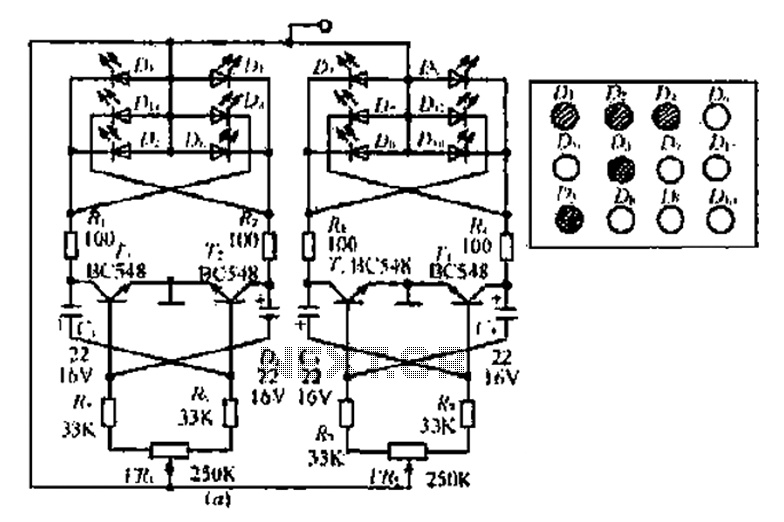
A circuit involving oscillations is composed of a Houle Wang oscillator that utilizes a transistor configuration with components labeled Ti, n, and n, along with a composition of Q constants for the cycle. The waveform can be modified by...
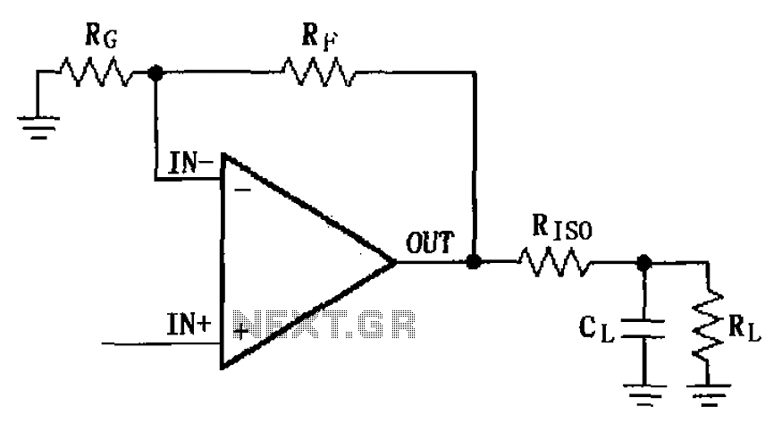
The MAX4223 to MAX4228 series incorporates a capacitive load drive circuit with an isolation resistor (RISO). The maximum allowable capacitive load for these devices is 25pF. However, exceeding this limit can lead to overshoot and ringing. The circuit design...
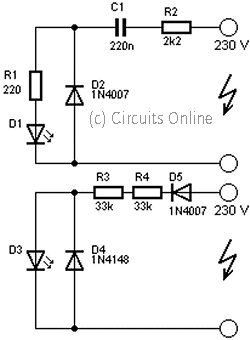
This circuit is used to power an LED with a voltage of 230V. The 230V must be reduced to meet the LED's voltage requirements. To achieve this, a circuit is necessary as described below. The circuit designed to power an...
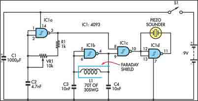
The circuit incorporates two oscillators, both operating at about 40kHz. The first, IC1a, is a standard CMOS oscillator with its frequency adjustable via VR1. The frequency of the second, IC1b, is highly dependent on the inductance of coil L1,...

As illustrated in FIG TDA4866, the circuit consists of an external signal generator circuit protection. The internal protection circuit's role is to manage control, while the external protection circuit performs its functions. During normal operation, the vertical amplitude of...
This generator circuit utilizes an overdriven amplifier to generate a 60 Hz square wave from the 60 Hz AC line. The circuit is suitable for line-operated applications as a clock source. The generator circuit operates by leveraging an overdriven amplifier...