
Microphone-Controlled Voice-Activated Switch

The circuit begins with an electret microphone, which serves as the audio input source. The microphone generates an analog audio signal that is routed to a bandpass filter circuit (IC1A). This filter is designed to allow only a specific range of frequencies to pass through while attenuating frequencies outside this range, thereby enhancing the quality of the audio signal for further processing.
Following the bandpass filter, the filtered audio signal is sent to a comparator. The purpose of the comparator is to compare the incoming audio signal against a reference voltage, determining whether the audio signal exceeds this reference level. When the audio signal is sufficiently strong, the comparator output transitions, activating the subsequent stage of the circuit.
The output of the comparator drives Q1, which functions as a switch. When Q1 is activated, it allows current to flow through the circuit. The conduction of Q1 is influenced by the components D1, C4, R6, and R7. D1 is likely a diode that ensures current flows in one direction, providing protection against reverse polarity. Capacitor C4 may serve to filter out high-frequency noise, while resistors R6 and R7 are likely involved in setting the biasing levels for Q1, ensuring it turns ON when the audio signal from IC1B is present.
This arrangement creates a responsive system that activates Q1 based on the presence of audio signals, allowing for further control or processing of the audio input as required by the overall application. The design effectively integrates the microphone, filtering, comparison, and switching elements into a cohesive audio processing circuit. An electret microphone feeds a bandpass filter circuit (IC1A), then feeds a comparator, which in turn drives Ql. Ql is a switch that conducts when audio from IC1B causes Dl, C4, R6, and R7 to bias it ON.
Related Circuits
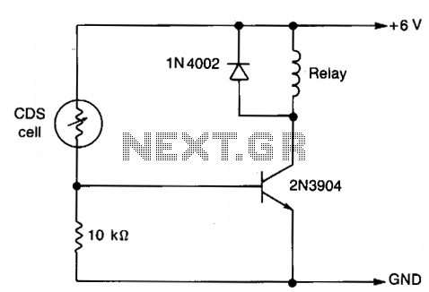
The resistance of the CDS cell decreases when exposed to light, activating the 2N3904 relay driver. The circuit utilizes a Cadmium Sulfide (CDS) photoresistor, which is a light-dependent resistor that changes its resistance based on the intensity of light...
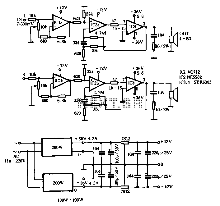
The T amplifier circuit schematic section is illustrated in Figure 3-51. It utilizes the Japan Sanyo STK6303 Pina, which is a high-power thick film integrated circuit. The maximum power supply voltage is 36V, and the output current can reach...
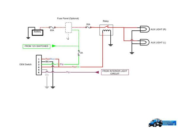
A schematic has been created to illustrate how the OEM AUX switch should be wired, providing a reference for installation. The switch pin layout is labeled for clarity when viewed from the terminals, with the locking tabs on the...
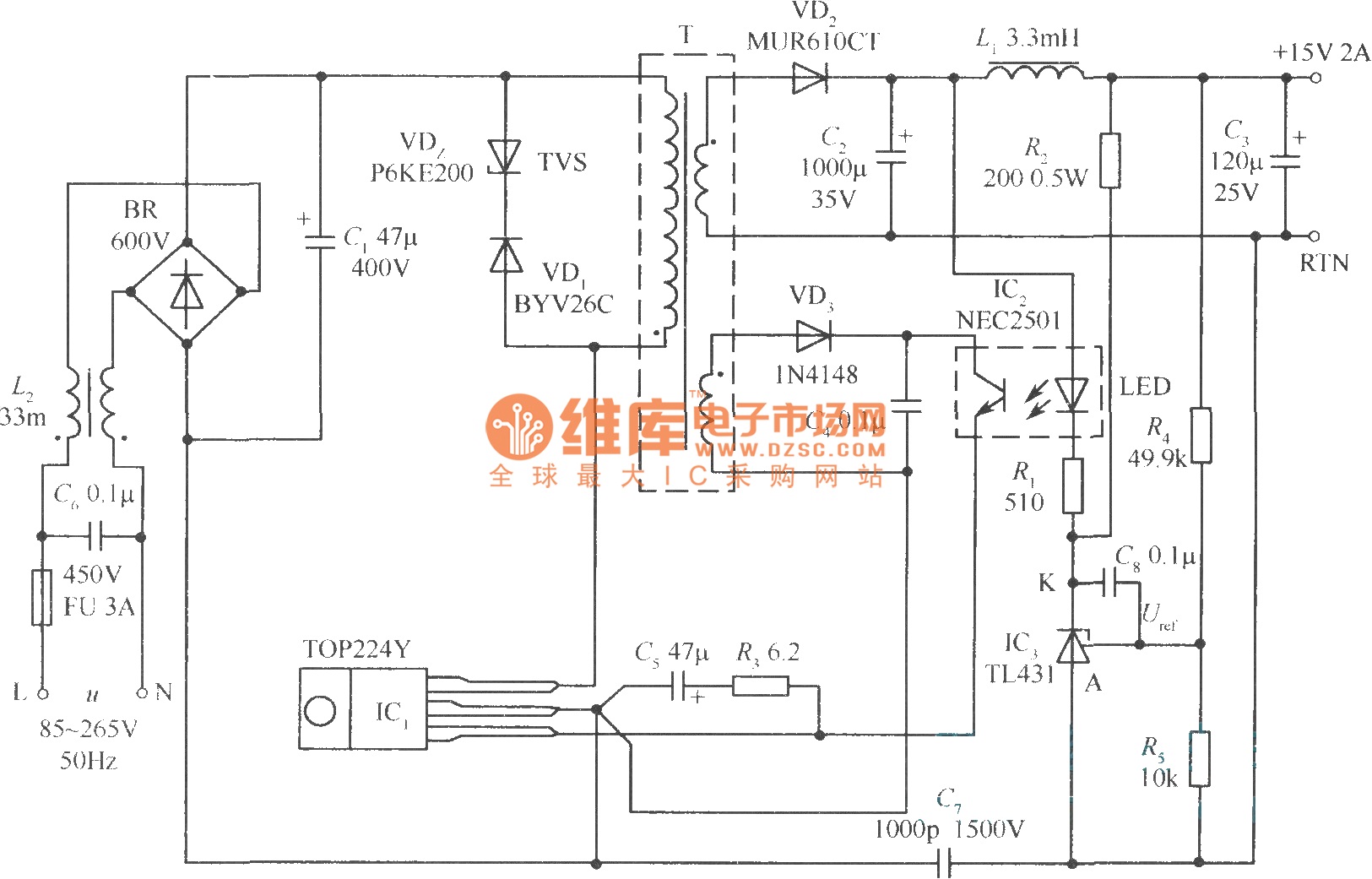
This document presents a 30W micro switch regulated power supply utilizing the TOP224Y integrated circuit. The circuit diagram illustrates its design. A notable feature of this power supply is the use of the TL431 component to replace the regulation...
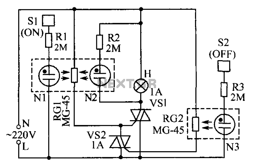
The circuit operates based on the principle that neon tubes N1, N2, and the photosensitive resistor RG1 form an optocoupler. When a finger touches the metal sheet S1, N1 lights up, causing RG1's resistance to decrease. This reduction allows...
Typically, a single telephone is connected to a telephone line. If an additional telephone is needed at a distance, a parallel line is installed for connecting the second telephone. This straightforward parallel line arrangement presents issues such as loss...