
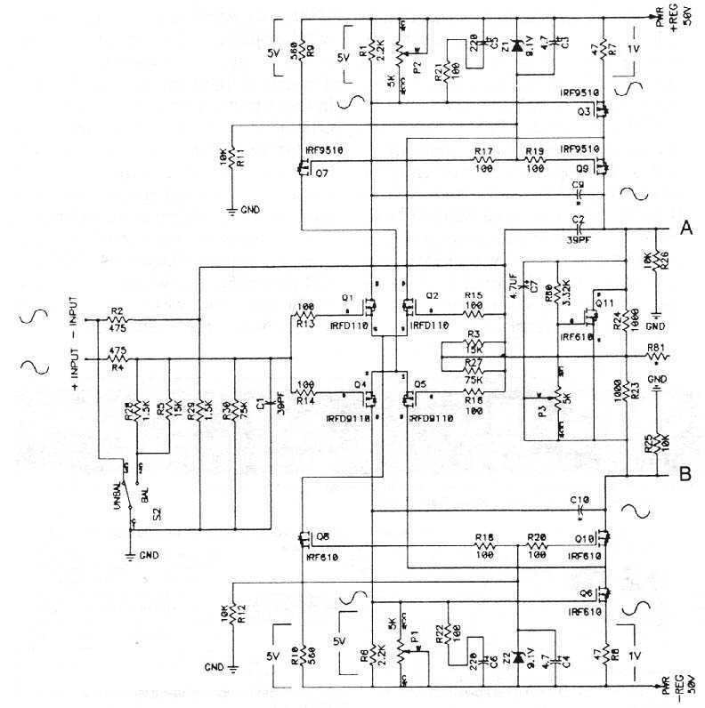
Mosfet 75W Power Amplifier
In both N- and P-channel it is of interest to know at what rate the current will change with respect to the gate-to-source voltage. This figure is called the transconductance, and tells you how much change in current to expect for a change in gate voltage. It is generally expressed as mhos (the opposite of ohm), because it describes a reversal of resistance. An ohm is volts divided by amps, and a mho is amps divided by volts, so that transconductance is defined as change of current for a change of control voltage. A device having one mho transconductance will increase its current by 1A for each additional volt on the gate.
Two more points are of interest. First, the MOSFET's construction provides for a reverse bias diode across the drain to source pins, which occasionally is convenient. The second point is rather important from a reliability standpoint: a rather strict limit specifies how much voltage you can apply to the gate before it will break. In our MOSFETs the limit is about 20V. Exceed it and you will need another MOSFET. Static discharge is an excellent way to exceed the limit, and the best way to do that is to pick a cold and dry winter day, shuffle across the nylon carpet in your rubber shoes, and touch the gate of a MOSFET. The second best way is simply to forget to touch earth ground before you touch that part for which you do not have a spare.
That's most of what there is to know. Other reliability details include rated voltage, current and wattage, and what package the MOSFET is in, but you can see these in the catalog. More arcane bits of information include saturation resistance, various capacitances, switching times and such, but if you can remember the preceding description you know 90% of everything about MOSFETs, and 100% of what you need to understand this project.
The N-channel and P-channel MOSFETs are essential components in modern electronic circuits, functioning as switches or amplifiers. The N-channel MOSFET allows current to flow from the drain to the source when the gate voltage exceeds the threshold voltage, typically around 4V. This characteristic makes it suitable for low-side switching applications, where the load is connected to the positive supply, and the MOSFET is used to ground the load when activated. Conversely, the P-channel MOSFET operates with reversed polarities, allowing current to flow from the source to the drain when the gate voltage is sufficiently negative relative to the source. This makes it appropriate for high-side switching applications, where the load is connected to ground and the MOSFET connects the load to the positive supply when activated.
Transconductance is a critical parameter, indicating how effectively a MOSFET can control current flow with changes in gate voltage. It is essential for designing amplifiers and switching circuits, as it determines the gain and response time of the device. The reverse bias diode integrated into the MOSFET structure provides additional protection against voltage spikes and can be utilized for inductive load applications, where back EMF could otherwise damage the device.
Careful consideration of the maximum gate voltage rating is necessary to ensure reliable operation. Exceeding the specified limit, usually around 20V for many MOSFETs, can lead to catastrophic failure. Proper handling and grounding techniques are crucial to prevent static discharge damage, which can occur easily in dry environments. Additionally, understanding the thermal characteristics, including power dissipation and junction temperature, is vital for maintaining the longevity and reliability of the MOSFET in circuit applications. Overall, MOSFETs are versatile devices that play a crucial role in electronic design, requiring a solid understanding of their operational principles and specifications for effective implementation in various applications.The MOSFETS we are dealing with are three terminal devices which are used to control electron flow in a circuit. Two of the pins (the source and drain) pass the current, and the third pin (the gate) is used to control the current.
The control of current, as seen from the outside, is accomplished by placing a voltage on the gate relative to the source pin. In the case of the N- Channel MOSFET, which approximates tube operation, increased current flows from the drain through the source in response to positive gate voltage, with respect to the source voltage (fig.
2b) If you wish more current, make the gate-to- source voltage more positive (for less, make it less positive). Conduction in the N-channel MOSFET will start generally at about 4V: less than 4V, no current; more than 4V, current flows.
The N-channel type's opposite number is the P-channel type, which is the same but with all the voltage polarities reversed. The drain is generally at a negative voltage with respect to the source, and current flows as the gate voltage becomes negative with respect to the source (Fig.
2b). In both N- and P-channel it is of interest to know at what rate the current will change with respect to the gate-to- source voltage. This figure is called the transconductance, and tells you how much change in current to expect for a change in gate voltage.
It is generally expressed as mhos (the opposite of ohm), because it describes a reversal of resistance. An ohm is volts divided by amps, and a mho is amps divided by volts, so that transconductance is defined as change of current for a change of control voltage.
A device having one mho transconductance will increase its current by 1A for each additional volt on the gate. Two more points are of interest. First, the MOSFET's construction provides for a reverse bias diode across the drain to source pins, which occasionally is convenient.
The second point is rather important from a reliability standpoint: a rather strict limit specifies how much voltage you can apply to the gate before it will break. In our MOSFETs the limit is about 20V. Exceed it and you will need another MOSFET. Static discharge is an excellent way to exceed the limit, and the best way to do that is to pick a cold and dry winter day, shuffle across the nylon carpet in your rubber shoes, and touch the gate of a MOSFET.
The second best way is simply to forget to touch earth ground before you touch that part for which you do not have a spare. That's most of what there is to know. Other reliability details include rated voltage, current and wattage, and what package the MOSFET is in, but you can see these in the catalog.
More arcane bits of information include saturation resistance, various capacitances, switching times and such, but if you can remember the preceding description you know 90% of everything about MOSFETs, and 100% of what you need to understand this project. 🔗 External reference
Related Circuits
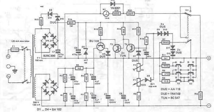
A DC power supply can be designed using high voltage transistors to provide an adjustable supply voltage ranging from 10 to 300 volts, which can be modified with potentiometer P1. Transformers used in these power supplies typically feature multiple...

A common emitter amplifier is a total pole amplification circuit structure featuring a key emitting device. This circuit refers to the emitter of the input signal and the output signal connected to a common ground, forming the basis of...

Designs for audio amplifiers with DC coupling to the load are not commonly seen today, despite their clear benefits. One advantage... Audio amplifiers utilizing DC coupling to the load present several notable advantages in specific applications. DC coupling allows for...
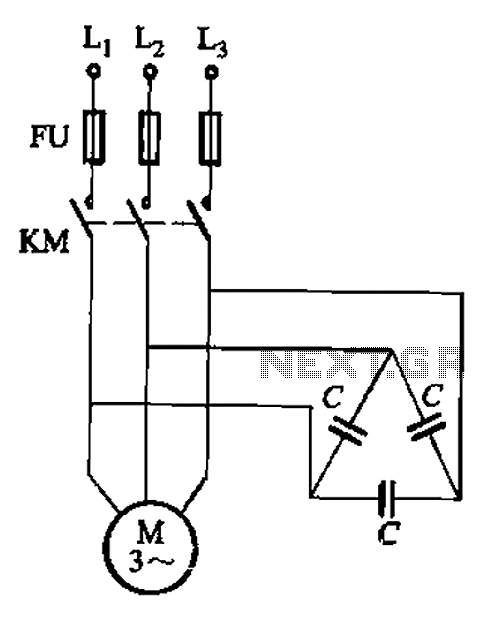
Asynchronous motor reactive power compensation involves directly connecting a capacitor to the stator windings of the asynchronous motor to enhance its power factor. This method is particularly effective for synchronous motors, as it reduces energy consumption related to reactive...
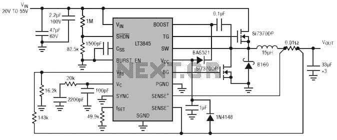
Burst Mode operation maintains high efficiency at light loads by reducing IC quiescent current to 120 µA. Light load efficiency is also improved with the reverse inductor current inhibit function, which supports discontinuous operation. Additional features include an adjustable...
Medical and industrial applications often require galvanic isolation of 2500 V AC or higher for the safety of patients and equipment operators. The isolation barrier conveys not only power to the sensing element but also data to or from...