
mosfet voltage regulator

The MOSFET-based linear voltage regulator described operates by utilizing the IRF540 N-channel MOSFET to regulate output voltage effectively while maintaining low voltage drop across the device. The circuit's design is centered around the principle of maintaining a stable output voltage through the feedback mechanism provided by the TL431 adjustable shunt regulator. This component monitors the output voltage and adjusts the gate voltage to the MOSFET accordingly, ensuring that the output remains within the desired specifications.
The voltage doubler circuit plays a crucial role in providing the necessary gate drive voltage. The configuration of diodes D1 and D2, alongside capacitors C1 and C2, allows the circuit to generate a higher voltage for the gate than the source, which is essential for fully turning on the MOSFET and minimizing its on-resistance (Rds(on)). This is particularly important for achieving the low voltage drop characteristic of the regulator.
The inclusion of a heatsink for the MOSFET is critical when operating at higher currents. The circuit can handle up to 3A output, but thermal management must be considered to prevent overheating and ensure reliability. The use of trimpot VR1 for output voltage adjustment allows for fine-tuning, accommodating variations in component tolerances and ensuring precise regulation.
The crowbar protection mechanism is an essential safety feature, designed to protect the circuit during output short-circuit conditions. By utilizing a combination of capacitors and diodes, the circuit can quickly respond to a drop in output voltage, activating the MOC3021 optocoupler to limit the gate voltage and thus the output current. This feature enhances the robustness of the design, making it suitable for various applications where accidental shorts may occur.
Overall, the MOSFET-based linear voltage regulator is a versatile and efficient solution for applications requiring stable voltage regulation with low dropout characteristics. Its design allows for adaptability in component selection and configuration, making it a valuable addition to any electronics project requiring precise voltage control.It can be simplified and you can leave out short-circuit protection if you wish. This circuit is a Mosfet-based linear voltage regulator with a voltage drop of as low as 60mV at 1A. The circuit uses a 15V-0-15V transformer and employs an IRF540 N-channel Mosfet (Q1) to deliver the regulated 12V output. The gate drive voltage required for the Mosfet is generated using a voltage doubler circuit consisting
of diodes D1 & D2 and capacitors C1 & C2. To turn the Mosfet fully on, the gate terminal should be around 10V above the source terminal which is connected to the DC output. The voltage doubler feeds this voltage to the gate via resistor R3. IC2, a TL431 adjustable shunt regulator, is used as the error amplifier. It dynamically adjusts the gate voltage to maintain the regulation at the output. With an adequate heatsink for the Mosfet, the circuit can provide up to 3A output at slightly elevated minimum voltage drop.
Trimpot VR1 is used for fine adjustment of the output voltage. The RC network consisting of R5 and C6 provides error-amplifier compensation. The circuit is provided with short-circuit crowbar protection to guard against an accidental short at the output. This crowbar protection works as follows: under normal working conditions, the voltage across capacitor C5 will be 6.
3V and diode D5 will be reverse-biased by the output voltage of 12V. However, during output short-circuit conditions, the output will momentarily drop, causing D5 to conduct. This triggers the MOC3021 Triac optocoupler (IC1) which in turn pulls the gate voltage to ground. This limits the output current. The circuit will remain latched in this state and the input voltage has to be switched off to reset the circuit.
I tested this circuit today and it works but I didn`t have irf540 but irf520. So i needed to tweak resistors r6, r7 and r8. And I left out short-circuit protection: r1, r2, zd1, c5, ic1, d5 and r4. And off cource you can use diode bridge rectifier, transformer with single secondary winding and I would use c3 and c4 low esr with higher value. I don`t know how good is this voltage regulator in comparison with Sigma11. I tested it with my mosfet amp and I noticed a bit strange colored sound. But I guess that is because that high Rds(on) off irf520. Or maybe it is how it should sound. I had 78s12 regulator and now I`m using lm317t which is a bit better and I believe with a bit more bass.
Edit: I`m currently using this regulator with 12V transformer and works great. Vin drops to 15, 9V, Vout is set to 15V (!) and Iout is 0, 5A. So no need for huge Vin-Vout voltage as with 7812, LM317T or other regulators. With higher input voltage is possible to remove c1, 2 and d1, 2 and r3 connect directly to input voltage on drain. I added c8 because I have right part of the schematic around 10cm further and it oscillated without it.
I know that it isn`t a good idea but I had a hole in heatsink and space in my case is somewhat limited. Resistors r6 and r8 determine output voltage: (1+r6/r8)x2, 5. For example: (1+5k6/1k5)x2, 5=11, 83. But it depends on real part values and adjust voltage of tl431. Now I have (1+7k5/1k5)x2, 5=15 and 15, 03 in reality. I was doing A/B testing for lm317 vs mosfet and frankly I was unable to hear any difference at all. But lm317 is better than 78s12. I`ll stick with this mosfet just because I`m a mosfet fan and it`s something new for me. It`s not surprising that you didn`t hear difference, LM317 has quite low noise, so noise from PSU was not present (was present, but under hearing threshol), PSRR of LM317 is also quite good and if your amp is all class A, then current drawn from PSU is constant, so high imedance of PSU doesn`t (can`t) degrade sound quality.
🔗 External reference
Related Circuits
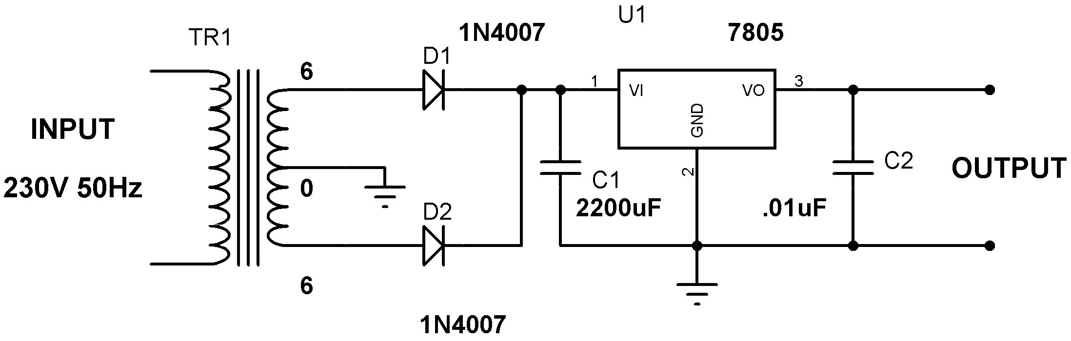
Designing a power supply requires careful consideration of each component. This discussion will focus on the design of a regulated 5V power supply. Note: Any transformer that provides a secondary peak voltage of up to 35V can be used;...

This is a variation of the astable multivibrator. The circuit was recently developed to test N-channel MOSFETs (such as the IRF830). The described circuit is an astable multivibrator configuration tailored specifically for testing N-channel MOSFETs, particularly power MOSFETs like the...
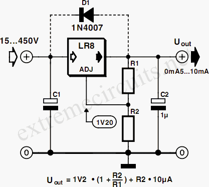
Commonly used 3-pin linear voltage regulators, such as the LM317, cannot handle input voltages exceeding approximately 30V. The LR8A from Supertex Inc is a new adjustable three-pin regulator capable of accepting input voltages up to 450V and supplying an...
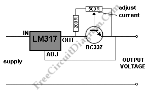
This is an adjustable constant current regulator circuit. This circuit can be used in a bench power supply to prevent the circuits that are tested from being damaged. The adjustable constant current regulator circuit is designed to provide a stable...
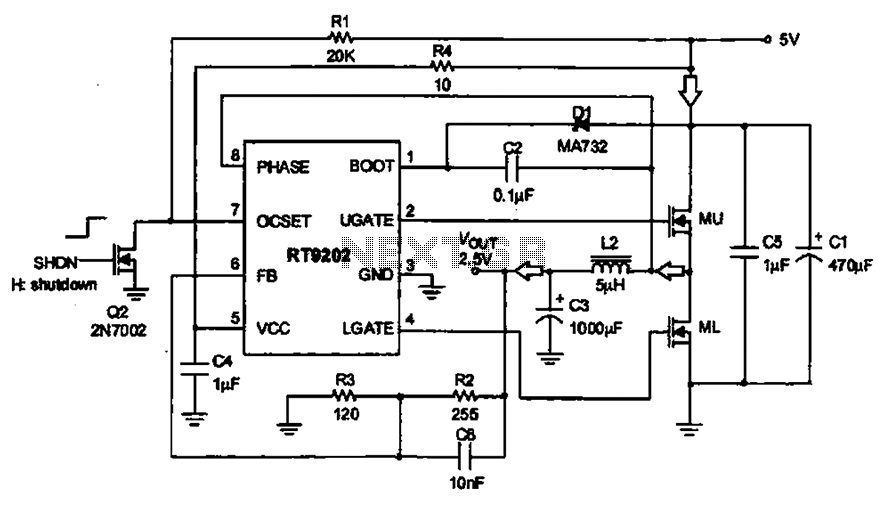
A 5V to 2.5V voltage regulator circuit is designed for use in computer motherboards. At its core, this circuit utilizes the RT9202 power management chip. The RT9202 functions as a switching pulse generating circuit, which, upon startup, converts a...
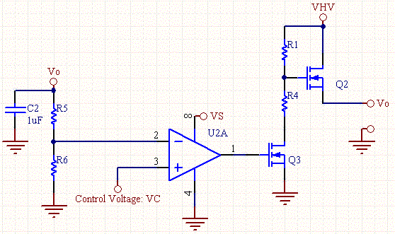
The drawback of the circuit mentioned is that the operational amplifier (op-amp) supply is connected to the high voltage (HV) supply. Most op-amps are limited to approximately 30V for their supply voltage, which prevents the circuit from functioning with...