
MOSFETs and CMOS Inverter

The evaluation of the first-order MOSFET theory through practical application involves a systematic approach to understanding the operational characteristics of n-MOSFETs and p-MOSFETs in the ALD1105 IC. The four-terminal configuration of the transistors allows for comprehensive analysis of their electrical behavior under different biasing conditions. The shared body configuration of the n-MOSFETs and p-MOSFETs necessitates careful attention to voltage levels to prevent undesired conduction through the body diode, which can compromise device performance.
The construction of the CMOS inverter serves as a practical application of MOSFET theory, enabling the demonstration of voltage-controlled switching. The function generator's output settings play a crucial role in ensuring that the inverter operates correctly, with specific attention to the DC offset and peak-to-peak voltage. The determination of threshold voltage, maximum drain current, and other critical parameters from the datasheet is essential for predicting the inverter's behavior under various operating conditions.
The process of measuring the I-V characteristics using a 2-wire analyzer provides valuable insights into the transistor's performance, particularly in identifying the threshold voltage where the device transitions from the off state to the on state. This measurement is vital for verifying the specifications outlined in the datasheet and ensuring that the transistors function as intended in the circuit. The careful analysis of current readings, especially at low levels, highlights the limitations of measurement equipment and the importance of accurate data interpretation in the context of semiconductor device characterization.Using measured threshold voltage and Ids-Vds curves, we can then check how well first-order MOSFET theory holds up in real devices and get a practical feel of the limitation of first-order theoretical MOSFET equation. The MOSFETs we will use in this experiment are from ALD1105, an IC containing two n-MOSFETs and two p-MOSFETs.
A circuit symbol des cription of the two pairs of transistors from the data sheet is shown below in figure 1. Note each transistor has four terminals: drain (D), source (S), gate (G), and substrate, which is called body (B) in our text. As we learned in class, all the n-MOSFETs on an IC share the same p-type body, which needs to be tied to the lowest voltage in a system to keep all the source/drain to body PN junctions zero or reverse biased.
Similarly, all the p-MOSFETs on an IC share the same n-type body, which needs to be tied to the highest voltage in a system to keep all the source/drain to body PN junctions zero or reverse biased. A MOSFET is a natural voltage-controlled switch, as illustrated in figure 3. A high gate voltage turns on the MOSFET channel, allowing current to flow between drain and source, thereby turning a load, which can be a LED, a speaker or a fan.
The amount of current the MOSFET can provide depends on the transistor physical properties such as width, length, oxide thickness, etc. , the gate voltage, and the load. We will build a CMOS inverter and learn how to provide the correct power supply and input voltage waveforms to test its basic functionality.
For a given supply VDD, your voltage low should be zero, and voltage high should be VDD. By default, the function generator gives an output that varies from -VPP/2 to +VPP/2, with VPP being peak-to-peak voltage. For a square wave, the voltage low is -VPP/2, voltage high is +VPP/2. You can set the DC offset to VPP/2 to make voltage low 0. Using the datasheet, determine the values of the threshold voltage range, the maximum continuous drain current ID, the maximum drain-source voltage, and the maximum allowed power dissipation, Ptot.
For a VDD of 3V, 5V, 7V, sketch the input waveforms required to test the functionality of the CMOS inverter. Determine the VPP and dc offset setting required for function generator. On the data sheet, the threshold voltage is defined to be the value of Vgs when ID = 1 uA when the transistor is biased at saturation.
The data sheet uses the notation Vgs(th) for the threshold voltage, whereas our text uses the notation Vtn. We can force a transistor to work in saturation by connecting the drain and gate. We can then measure the I-V curve of this diode-like circuit using the 2-wire analyzer. The threshold voltage can then be determined from the voltage at which current equals a set threshold.
In the 2-wire SFP select the Cursor On box. This will allow you to see the current and voltage values at specific points. Using this check the voltage value at the point where Id = 1uA. Does your value of Vtn fall within the range specified on the data sheet As you can see from the screen shots provided below, some significant figures are lost on the y-axis as very small current readings are measured. This is the result of the ELVIS II unit measuring correct values but the y-axis being unable to display below a certain threshold.
🔗 External reference
Related Circuits

Adjust the potentiometers RPi and RPz to modify the speed of two motors. The circuit utilizes two potentiometers, designated as RPi and RPz, to control the speed of two separate motors. Each potentiometer is connected in a voltage divider configuration,...
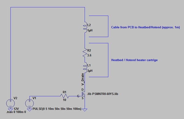
The primary concern is that the RDS_on of the utilized MOSFETs, when driven with a 5V gate voltage, is excessively low. Additionally, the reverse voltage that occurs when the MOSFET transitions from the on to the off state can...

Using this circuit you can convert the 12V dc into the 220V AC. In this circuit, 4047 is used to generate the square wave of 50Hz and amplify the current and then amplify the voltage by using the step...

The circuit below uses a CMOS dual D flip flop (CD4013) to toggle a relay or other load with a momentary push button. Several push buttons can be wired in parallel to control the relay from multiple locations. A...
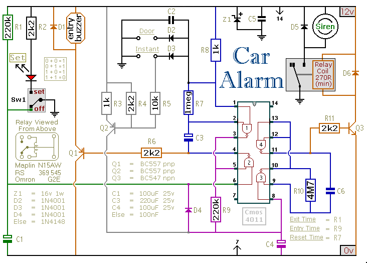
This car alarm circuit includes exit and entry delays, an instant alarm zone, an intermittent siren output, and automatic reset. By incorporating external relays, it is possible to immobilize the vehicle and activate the flashing lights. The car alarm circuit...
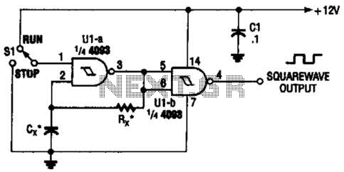
Two gates of the Quad 4093 are utilized to create an oscillator. The resistor (R) can range from approximately 5 kΩ to around 10 kΩ. The capacitor (Cx) can vary from about 10 pF to higher values, with the...