
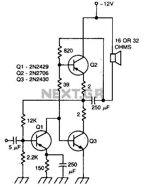
N-Power Amplifier

The input stage features a differential pair with a constant-current source in the tail and resistor loading. The PCB includes tracks and pads for implementing a current mirror for future upgrades. The voltage amplifier stage (VAS) employs a bootstrap capacitor to function as a current source, allowing the drive to the upper output device to swing above the positive supply rail, thereby enhancing efficiency. The lower output device is configured as a Sziklai pair, which also contributes to good efficiency. The bias generator (T6, R11, P1, R12) is designed such that if the potentiometer becomes open circuit, the bias current will decrease to a minimal level. Zener diodes are placed on the MOSFETs to protect against over-voltage conditions that could damage the gate. Corresponding diodes in series prevent any back EMF from the load from inadvertently turning on the MOSFET.
It is crucial not to apply power to the amplifier until the bias transistor and output devices have been mounted to the heatsink, as failure to do so may destroy the output devices. Fuses should not be installed initially; instead, 100-ohm, 1-watt resistors should be used in their place. These "safety resistors" will limit current in the event of a fault and prevent damage to the amplifier. Fuses may not react quickly enough in case of a build error. The bias preset potentiometer should be turned fully anti-clockwise without force. To check the setting before soldering it to the PCB, position the preset potentiometer so the middle pin is higher than the outer pins. Measure the resistance between the middle pin and the rightmost pin; it should be less than 50 ohms. An ammeter should be connected in series with the negative rail. Upon applying power, the reading on the ammeter should be less than 20 mA, and the "safety resistors" should remain cool. If either condition is not met, power must be removed immediately, and the bias preset potentiometer should be verified to be set to minimum. If confirmed, inspection for solder bridges, broken tracks, dry joints, and incorrect components should be conducted.
Once everything appears satisfactory, the bias preset potentiometer can be adjusted clockwise to see an increase in current. The target is to set it to 75 mA, monitoring the current every minute to ensure it does not exceed 100 mA within 2 minutes; if it does, it should be reduced back to 75 mA. Some fluctuation may occur as thermal equilibrium is achieved, typically within about 15 minutes, depending on the heatsink. Connecting a loudspeaker or playing signals should not be attempted during this period, as the "safety resistors" will prevent the amplifier from functioning in that manner. After setting the bias current, the output of the amplifier should be checked to ensure that the DC offset is less than 50 mV. If it exceeds 1 V, a fault exists within the amplifier, necessitating a check for solder bridges, broken tracks, dry joints, and incorrect components. Once all checks are completed, power can be removed, and the "safety resistors" can be replaced with the correct rating fuses. The bias procedure should then be rechecked, as the bias current may increase slightly once the resistors are removed from the rail.The amp has been designed to be an ideal upgrade for builders wishing to step up from Gainclones. This amp will kick out the power where Gainclones fall over, yet still maintain a sweet sound. The use of n-channel MOSFETs in the output makes the amp easy to source parts for as well as being very rugged. Provided that high power MOSFETs such as the specified IRFP250 are used and the appropriate fuses are used on the board, the amp should shrug off short circuits at the output. With the recommended supply voltage of 41 V per rail (30 V transformer secondaries), 160 W RMS into 4 ohms is achievable, again if the recommended IRFP250 devices are used.
The use of less powerful MOSFETs will mean you need to use higher load impedances and/or reduce the rail voltage. A differential pair is used at the input, which features a constant-current source in the tail and resistor loading.
There are tracks and pads on the PCB to implement a current mirror for future upgrades. The voltage amplifier stage (VAS) uses a bootstrap capacitor to act as a current source, primarily to allow the drive to the upper output device to swing above the positive supply rail to increase efficiency. The lower output device is run as a Sziklai pair so has quite good efficiency too. The bias generator (T6, R11, P1, R12) is configured so that if the potentiometer goes open circuit, bias current will fall to a small amount.
The Zener diodes on the MOSFETs are to protect them from over-voltage which can `punch through` the gate destroying the device. The corresponding diodes in series with them prevent any back EMF from the load turning the MOSFET on.
Do not apply any power to the amplifier until the bias transistor and output devices have been mounted to the heatsink. Failure to do this will most likely destroy the output devices. Do not fit the fuses, instead fit 100 ohm 1 watt resistors in their place. These `safety resistors` will limit current in the event of a fault and prevent the amplifier blowing up.
Fuses will not act quick enough if there has been a build error. Turn the bias preset potentiometer as far anti-clockwise as possible, do not force it. If you wish to set and check this prior to soldering it into the PCB, orient the preset potentiometer so that the middle pin is higher than the outer pins. Now measure the resistance between the middle pin and the rightmost pin, it should be less than 50 ohms.
Connect an ammeter in series with the negative rail. Apply power and note the reading on the ammeter, it should be less than 20mA. The `safety resistors` should also be cool. If either of these is not true, remove power immediately and check the bias preset potentiometer is wound to minimum. If it is then begin to look for solder bridges, broken tracks, dry joints and wrong components, etc. If all seems OK then proceed to turn the bias preset potentiometer clockwise and you should see the current increase.
Set it to 75mA then keep checking the current every minute to make sure it is not running away - it should not reach 100mA within 2 minutes, if it does then turn it down to 75mA again. There will be some movement whilst thermal equilibrium is reached so do not worry too much. Thermal equilibrium should be reached by about 15 minutes, depending on the heatsink. Do not attempt to connect a loudspeaker or play any signals as the `safety resistors` will prevent the amplifier working in this way.
Once the bias current has been set you can check the output of the amp to make sure that the DC offset is less than 50mV. If it is more than 1V then there is a fault with the amplifier so check for solder bridges, broken tracks, dry joints and wrong components, etc.
Now that everything has been checked you can remove power and replace the `safety resistors` with the correct rating fuses and re-check the bias procedure above (the bias current will raise a little due to no longer having resistors in the rail 🔗 External reference
Related Circuits
This circuit exhibits less than 2% distortion and maintains a flat response within 3 dB from 15 Hz to 130 kHz. The described circuit is engineered to provide high fidelity audio performance, characterized by minimal distortion and a wide frequency...
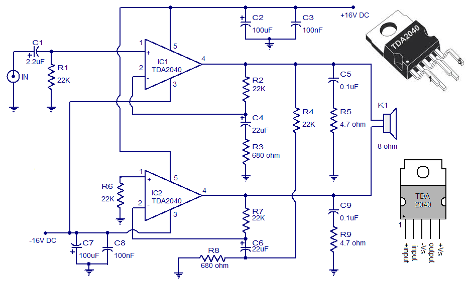
A 30 Watt audio amplifier circuit utilizing the TDA2040 is illustrated here. The TDA2040 is a class AB monolithic integrated audio amplifier available in a Pentawatt package. This integrated circuit features low harmonic distortion, minimal crossover distortion, and includes...
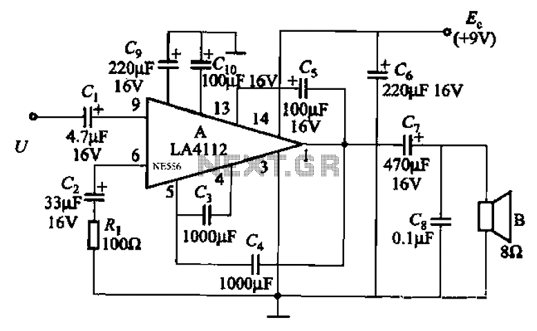
Audio power amplifier circuit utilizing the LA4112 integrated power amplifier along with additional components as shown in the figure. The audio power amplifier circuit based on the LA4112 integrated power amplifier is designed to deliver high-quality audio amplification for various...
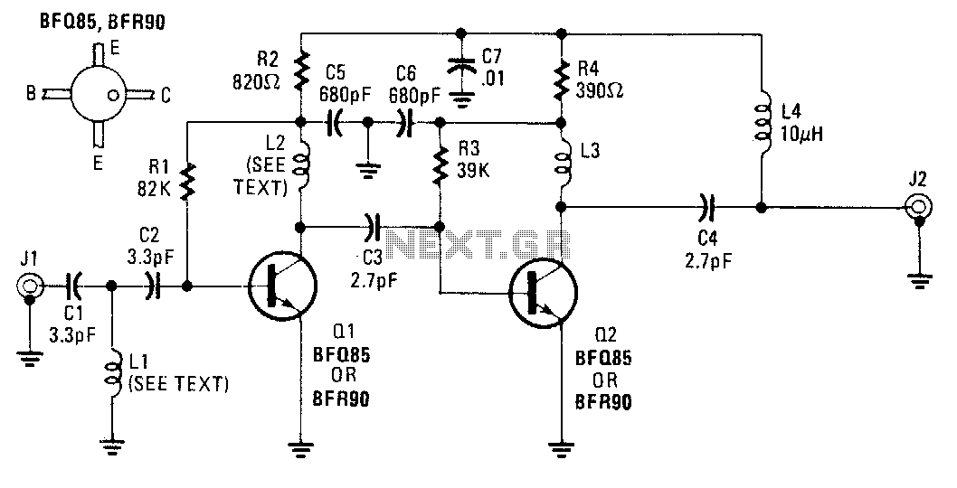
An inexpensive antenna-mounted UHF-TV preamplifier can add more than 25 dB of gain. The first stage of the preamplifier is biased for optimum noise performance, while the second stage is optimized for maximum gain. Additional details include Ll and...
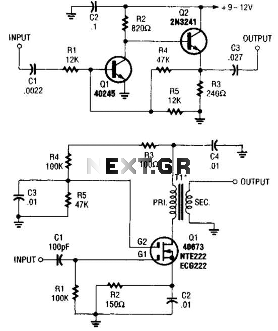
These two buffer/amplifiers have been effectively utilized with variable frequency oscillators (VFOs): one (depicted in A) is constructed using a pair of bipolar NPN transistors, while the other (illustrated in B) is designed around a dual-gate MOSFET. The first buffer/amplifier,...
A controllable gain amplifier functions as an automatic gain control circuit within the execution unit. The primary methods for controlling the amplifier's gain involve two approaches: one is by adjusting certain parameters of the amplifier itself, such as emitter...