
Buffer Amplifiers Circuit

The first buffer/amplifier, utilizing bipolar NPN transistors, operates by providing high input impedance and low output impedance, which is essential for interfacing with sensitive components like VFOs. The circuit typically includes two NPN transistors configured in a common emitter arrangement. The input signal is fed into the base of the first transistor, which amplifies the signal before passing it to the second transistor for further amplification. This configuration not only boosts the signal strength but also maintains signal integrity, minimizing distortion.
The second buffer/amplifier, based on a dual-gate MOSFET, offers advantages such as lower noise and higher bandwidth compared to its bipolar counterpart. The dual-gate configuration allows for enhanced control over the gain and frequency response of the amplifier. In this design, the input signal is applied to one gate of the MOSFET, while the second gate is used for gain control, allowing for fine-tuning of the amplifier's characteristics. This makes it particularly suitable for applications requiring precise signal manipulation, such as in VFO circuits.
Both designs are critical in ensuring that the output signals from VFOs remain stable and undistorted, which is vital for the performance of radio frequency systems and other applications where signal fidelity is paramount. The choice between the two configurations depends on specific application requirements, including desired frequency response, noise performance, and power consumption. These two buffer/amplifiers that have been successfully used with VFOs: one (shown in A) is based on a pair of bipolar npn transistors, and the other (shown in B) is built around a dual-gate MOSFET.
Related Circuits
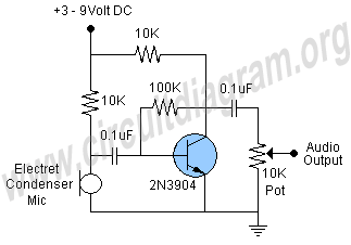
This schematic illustrates a highly sensitive microphone preamplifier circuit designed to amplify the gain of a microphone or enhance audio signals originating from a microphone. The circuit is straightforward, comprising only a few components, and can be assembled in...
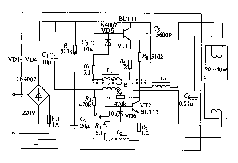
Electronic ballasts operate over a wide voltage range, provide fast startup with no noise or flicker, and contribute to energy savings. Their acceptance among users has been increasing. The circuit depicted in the figure represents a typical electronic ballast...
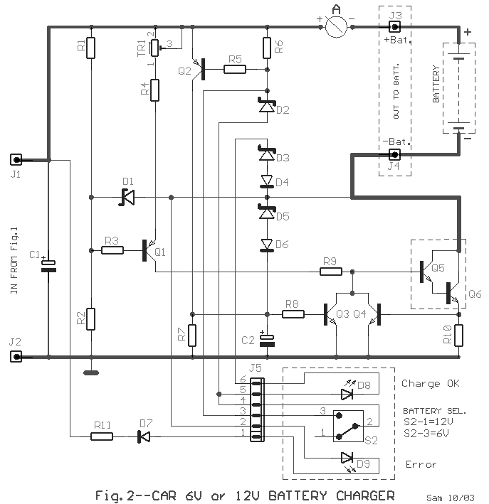
This circuit is capable of automatically charging 6V and 12V batteries quickly and accurately. A key factor in the successful operation of the circuit is the use of a high-quality transformer (T1) that features excellent insulation and short-circuit resistance. The...
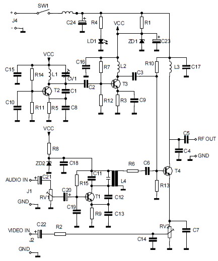
The circuit converts audio and video signals into a UHF TV signal, allowing a video signal from a camera or other source to be connected to a standard TV set. The audio and video signals are transformed into a...
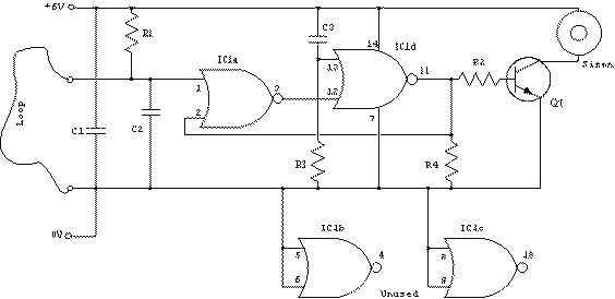
The loop can be any type of hookup wire, with a maximum resistance of about 90K. Using very thin wire (40AWG, for example) will create a highly sensitive trip wire, but will reduce the distance it can be strung...
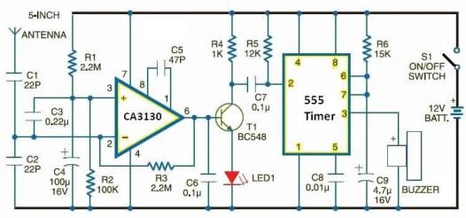
This electronic schematic allows for the design of a simple cellular phone detector circuit capable of sensing the presence of an activated mobile phone from a distance of 1.5 meters. The capacitor C3 should have lead lengths of 18...