
Nixie low voltage PSU

The described step-up converter circuit employs a 555 timer in astable mode to generate a square wave signal that drives a transistor switch. The transistor, in this case, the C945, is used to control the current flowing through the inductor L1, which stores energy during the "on" phase of the cycle. When the transistor switches off, the magnetic field around the inductor collapses, inducing a high voltage across the inductor according to the principles of electromagnetic induction.
The output voltage is determined by the turns ratio of the transformer or, in this case, the inductor and the configuration of the circuit. The diode D1 rectifies the high-frequency AC signal generated by the inductor into a DC output, which is then smoothed by a capacitor to provide a stable voltage. The trimmer R40 allows for fine-tuning of the output voltage by adjusting the duty cycle of the 555 timer, while R38 sets the timing characteristics of the circuit.
Overall, this circuit can be an effective solution for generating high voltages in small projects without the need for complex components, relying instead on widely available parts and straightforward design principles. Care should be taken during operation, as high voltages can pose safety risks. It is advisable to implement proper insulation and safety precautions while working with such circuits.Sometimes I need small high voltage power supply for my projects. And I don`t want to make special transformers. And I don`t want to use special chips for it. In internet I found very simple circuit diagram for classical step-up converter. It is base on very common 555 timer. The coil used in this schematics is bought in the shop. Some comments ab out this circuit diagram: I needed about 200V DC. During tuning I saw voltages going from Vin up to the voltage dangerous for diode, capacitor and mosfet. You only need to turn trimmer. Theoretical values are printed in this circuit diagram, but during constructed I didn`t managed to collect exact values and used components from my spare part box.
So here is comments about replacement of components: First of all, T1 is MPSA42. Why author used high voltage transistor Maybe he had lots of them. I don`t. The voltage here is only going to such level what 555 timer can handle- up to 18V. So I used more common transistor from computer power supply. It is C945 (50V, 0. 1A, npn) Trimmer R40 is 10K, R38- 470K. Diode D1 from old AT PSU, fast, high voltage diode FR154. L1 is from local hobby shop. They didn`t find any 100G H @ 1A, so I put 150G H. 🔗 External reference
Related Circuits
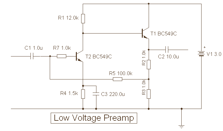
The provided description pertains to a unique low voltage variant of an audio preamp. The emitter voltage of T1 is biased close to half the supply voltage, which is 1.5V. This biasing allows for the maximum output voltage swing. The...
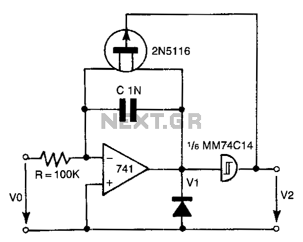
The 741 operational amplifier integrator signal is input into the Schmitt trigger of an inverter. When the signal reaches the positive-going threshold voltage, the inverter's output switches to zero. This output directly controls the FET switch. With a gate...
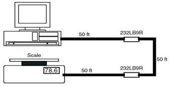
This is the schematic diagram of a 9-Pin RS232 Line Booster Signal Direction. The device functions as a 9-pin RS-232 repeater, re-transmitting all 8 signals while also maintaining the ground line. The 9-Pin RS232 Line Booster is designed to extend...
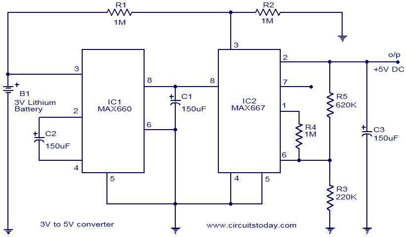
Voltage converter circuit diagram for converting 3 volts to 5 volts using CMOS monolithic ICs MAX660 and MAX667, which functions as a positive voltage regulator. The voltage converter circuit utilizes the MAX660 and MAX667 integrated circuits to step up a...
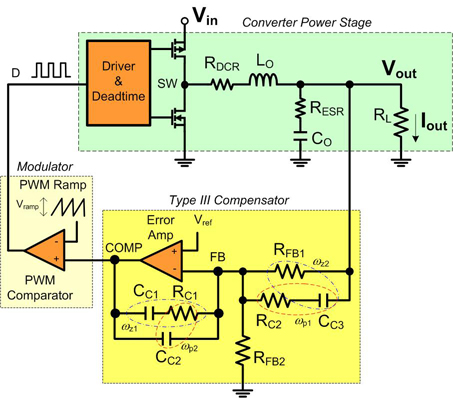
Before designing with one of today's powerful buck regulator ICs, it is essential to have a thorough understanding of voltage mode control and compensation. Voltage mode control is a widely used method in switching power supplies, particularly in buck converters....
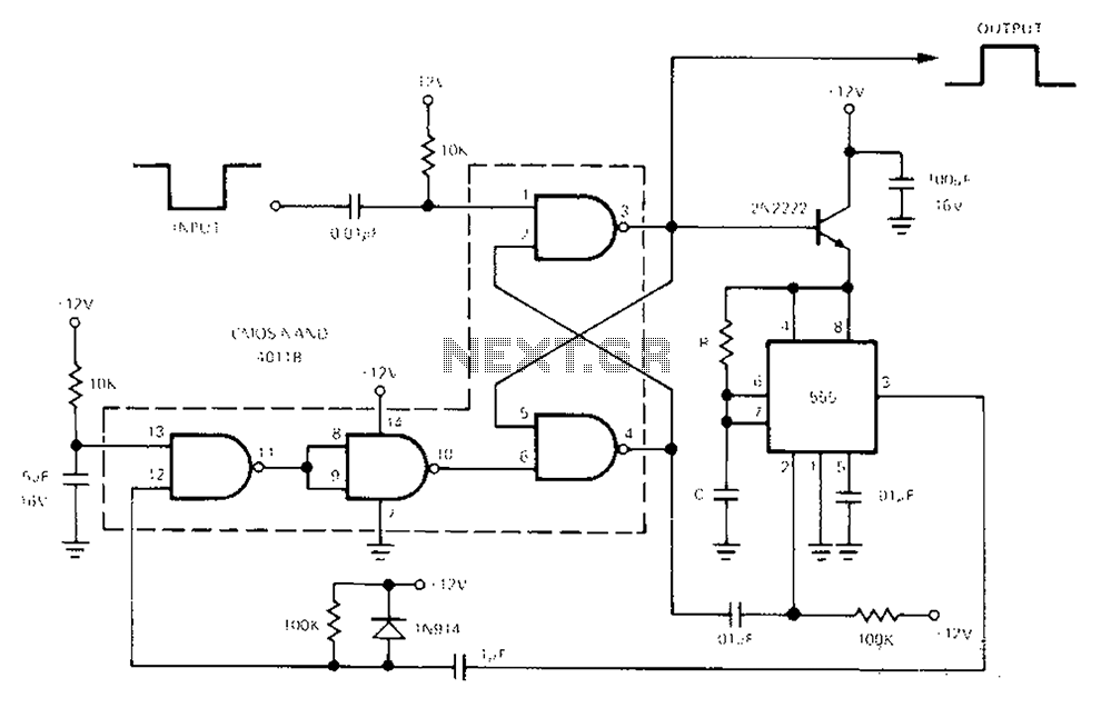
The 555 Timer facilitates a low-loss single-shot circuit and interfaces with the CMOS4011B NAND gate circuit. The standby power consumption is less than 50 µA. When the one-shot circuit is activated, the current consumption is 4.5 mA, and the...