
OCL Power Amplifier Circuit MJ15003MJ15004 Schematic Diagram

To ensure proper assembly, verify all components are correctly positioned, excluding the output transistors. Use a voltmeter to measure the voltage at the speaker terminals, ensuring it reads 0V or no more than 0.25V. If the voltage exceeds this range, circuit failure is indicated, necessitating further inspection. After verifying the output transistors, an ammeter should be used to measure the current with a shorted input circuit, adjusting VR1 to achieve a reading of approximately 20-40 mA. Transistor Q4 should be mounted on a heat sink to regulate bias current in relation to temperature changes. The bridge rectifier should be rated for at least 5A and 100V, while filter capacitors C7 and C8 should be 1000µF at 50V, resulting in a voltage of approximately 38V across the capacitors after filtering.
The circuit can be identified as an OCL power amplifier featuring MJ15003 and MJ15004 transistors.
This OCL 100W power amplifier circuit is designed for high-fidelity audio applications, utilizing a complementary push-pull output stage to deliver substantial power with minimal distortion. The direct coupling method enhances the amplifier's low-frequency response and overall sound quality by eliminating coupling capacitors that may introduce phase shifts or frequency roll-offs.
The input stage consists of Q1 and Q2, configured as a differential amplifier. This configuration provides high input impedance and excellent common-mode rejection, which is crucial for maintaining signal integrity in audio applications. The output from this stage is fed to Q5, a pre-driver stage that increases the signal level before it is sent to the driver stage (Q8 and Q9). This multi-stage amplification ensures that the final output stage can deliver the necessary power to drive speakers effectively.
The idle current is critical for the performance of the amplifier, as it affects the linearity and thermal stability of the output transistors. The adjustment of VR1 allows for fine-tuning of this current, ensuring that the output transistors operate within their optimal range, thereby reducing the likelihood of thermal runaway.
The output stage, consisting of Q10 and Q11, is responsible for delivering the amplified signal to the load (speakers). Proper heat dissipation is vital in this stage, as the output transistors can generate significant heat during operation. The inclusion of a heat sink for Q4, as well as the output transistors, is essential to maintain performance and reliability.
The power supply section, featuring a bridge rectifier rated for sufficient current and voltage, ensures that the amplifier receives adequate power to operate efficiently. The filter capacitors smooth out the rectified voltage, providing a stable DC supply to the amplifier circuit.
In summary, this OCL 100W power amplifier circuit is designed for high-performance audio applications, with careful consideration given to each stage of amplification, bias current control, and thermal management. Proper assembly and testing are crucial to ensure the amplifier operates as intended, delivering high-quality sound reproduction.This power amp OCL 100w is a very excellent sound quality. Since we provide the circuit in look All direct coupling form is connection join together direct all, to cut-off frequency low-loss problems, the super bass really do not tell who. The signal Input of the tone controls enter via C1 to the base pin of transistor Q1, which together with the
Q2 is differential amplifier, the signal from the collection pin of Q1 supplied to the bas pin of the Q5, which it acts as the pre-driver circuit. - The transistor Q4 is setting level bias or act as to control Idle current in this circuit. Which we can adjust level idle current by By adjusting the VR1. - The output signal from the Q5 will enter to base pin of Q8, Q9. which acts as the driver circuit. For the signal output to drive the output transistors Q10, Q11. -Check the assembly of all equipment to correct the circuit, without the output transistors, Using a voltmeter measure the voltage at the speaker.
By also does not have a speaker. At the end of this process was completed and ready to operate immediately. -Put the power supply to the circuit, then to measure the voltage is 0V or not higher than 0. 25V, if not in this means that the circuit failure, need to check first. -The later, on output transistors, and then use an ammeter to measure the current is supplied with short input circuit. Measuring that positive or negative wire. Then, adjust VR1 until reading about the current 20-40 mA. - For transistor Q4, when the device successfully. Should be installed on the cooling pad. Which installation of the output transistor. To help control the the bias current output relative to the temperature change of the output transistor.
- The Diodes Bridge rectifier should be not lower than 5 Amp 100V, The filter capacitor C7, C8 we used a 1, 000uF 50V, the voltage at the capacitor afer through the filter will can about 38V. You are reading the Circuits of OCL Power Amplifier Circuit MJ15003, MJ15004 And this circuit permalink url it is
🔗 External reference
Related Circuits
This device is a combination digital clock timer and solar panel charge controller designed to maintain a deep cycle battery charged by a solar panel. The timer output controls a 12-volt load for a 32-minute interval each day. The...
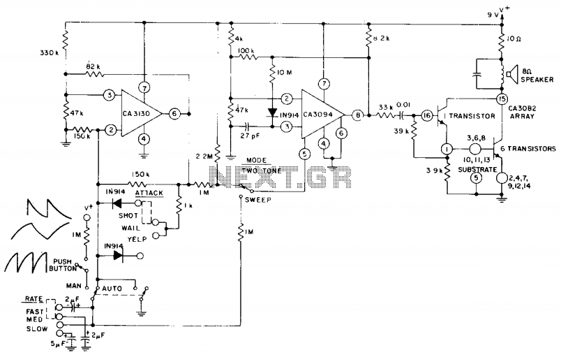
The circuit utilizes a CA3130 BiMOS operational amplifier configured as a multivibrator to regulate the siren's frequency. A CA3094 is employed as a voltage-controlled oscillator (VCO), which is subsequently connected to a CA3082 transistor array that drives a speaker....
The losses in a bridge rectifier can become significant when rectifying low voltages. The voltage drop across the bridge is approximately 1.5 V, which constitutes about 25% loss with an input voltage of 6V. This loss can be reduced...

A circuit diagram for an animal repeller is provided. The circuit has been developed but is not functioning as intended. Assistance is requested for troubleshooting. The animal repeller circuit typically employs ultrasonic sound waves to deter animals from specific areas....
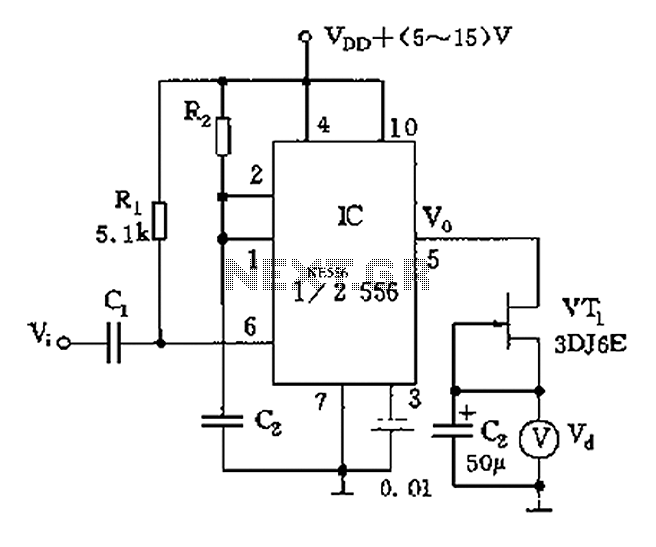
The circuit utilizes switch contacts that are proportional to the speed pulse signal Vi. A differential signal is fed into the trigger side of an integrated circuit (IC), specifically a 555 timer configured in monostable mode (1/2 556), to...

The TDA4935 is a bipolar stereo amplifier integrated circuit (IC) that can be configured as either a 2x15W stereo amplifier or a 30W mono BTL (Bridge-Tied Load) amplifier. This IC includes built-in circuitry for overload protection and over-temperature shutdown....