
Differential circuit with constant current
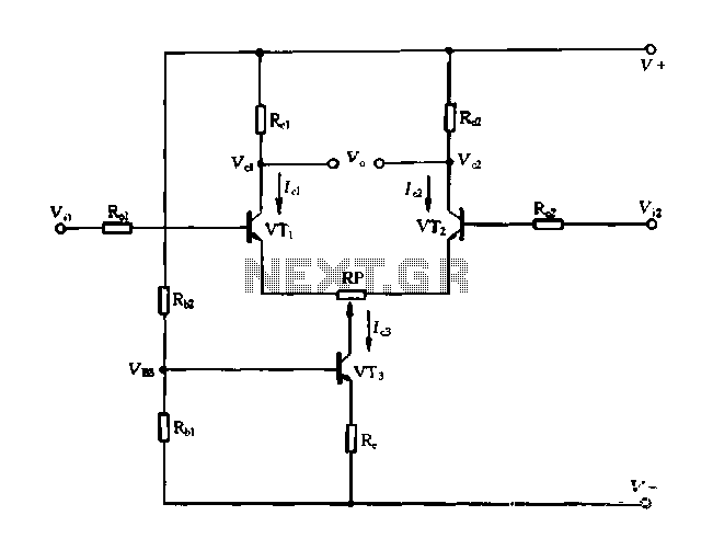
The differential amplifier with a constant current source is a critical component in analog signal processing. It operates by amplifying the difference between two input voltages while rejecting any signals that are common to both inputs, which is essential in minimizing noise and improving signal integrity. The arrangement of capacitors C1, C2, and C3 plays a vital role in stabilizing the amplifier's performance by controlling the bias currents and preventing drift due to temperature variations or component tolerances.
The four configurations for input and output processing allow for versatile applications, adapting the amplifier to various signal types and system requirements. The choice between single-ended and double-ended outputs influences the design of the subsequent stages in the signal chain, particularly in terms of impedance matching and noise considerations. The current mirror circuit, formed by transistors VT3 and VT4, is crucial for maintaining a stable output current, ensuring that variations in input signal amplitude do not adversely affect the amplifier's performance.
In practical applications, the differential amplifier is often used in instrumentation, audio processing, and communication systems, where precise signal amplification is required. The design considerations for such amplifiers include bandwidth, gain accuracy, and linearity, which are essential for maintaining fidelity in signal reproduction. The integration of a current mirror allows for improved performance by providing a consistent current source, thus enhancing the amplifier's dynamic range and overall efficiency.Differential amplifier with a constant current source, as shown in Figure 1-27. Thus, as long as, c3 and kept constant, cl, n can not be simultaneously increased or reduced sim ultaneously, thus inhibiting the voltage drift. Their differential circuit input signal, the output is divided into four different ways: double-ended input, double-ended output; double-ended input into a single-ended output; single-ended input, double-ended output; single-ended input, single-ended output. As shown in Figure 1-28. Magnification can be connected in four umbrella is: regardless of access method, as long as a single-ended output, the magnification of the basic amplification circuit half; if it is double-ended output, the magnification and the same basic amplifier circuit o differential amplifier circuit is almost always pre-stage amplifier circuit input section o Therefore, its output is always going to base this amplification circuit.
This single-ended output differential circuit is not a problem, while the double-ended output differential circuit would be inconvenient o because although it has two outputs, but not between the input signal and the common terminal, the single end output, you can not play to the advantages of the differential circuit. Hence the need for a double-ended to single output terminal matching circuit, which is the mirror current source circuit shown in Figure 1-29.
In Figure 1-29, VT3, VT4 constitute a mirror current source, therefore: Ic, 3 J d, and, c3 - Icl, so: Ic4 Icl output current D o Id - lc2 Icl - Ic2 0 when the common mode input (input terminal when two equal amplitude signals to common mode input), I {: 1 Ic2 so f. A, c2 0 and the same double-ended output. Differential input (two input terminal input equal in magnitude and opposite polarity signals, called differential mode input): Icl FIcl a Icl, Ic2 F, c2 + Ic2 because Icl F, spit so.
F2AlC. That differential input, the output current is a single-tube double current output, and also double-ended output the same. In the example above the circuit schematic will encounter later.
Related Circuits

Lead acid battery charger schematic using IC LM317. This lead acid battery charger circuit is simple to build and can be fit in a small box. The lead acid battery charger circuit utilizing the LM317 integrated circuit (IC) is a...
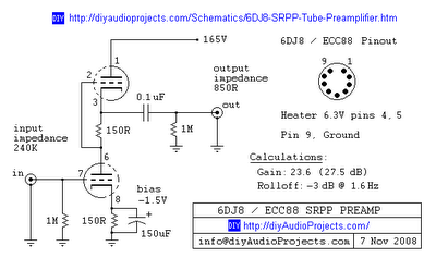
This is one of many available variations for a Symmetrical SRPP Preamplifier based on the 6DJ8 / ECC88 family of tubes. The SRPP circuit has also been referred to as a SEPP, Totem Pole, Mu Follower, Mu amplifier, and...

The circuit diagram illustrates the original Kodak MAX Flash Unit, including the semiconductors that comprise the circuit. This diagram represents the unmodified version intended for the standard Kodak model, which should closely resemble the Kodak MAX model, if not...
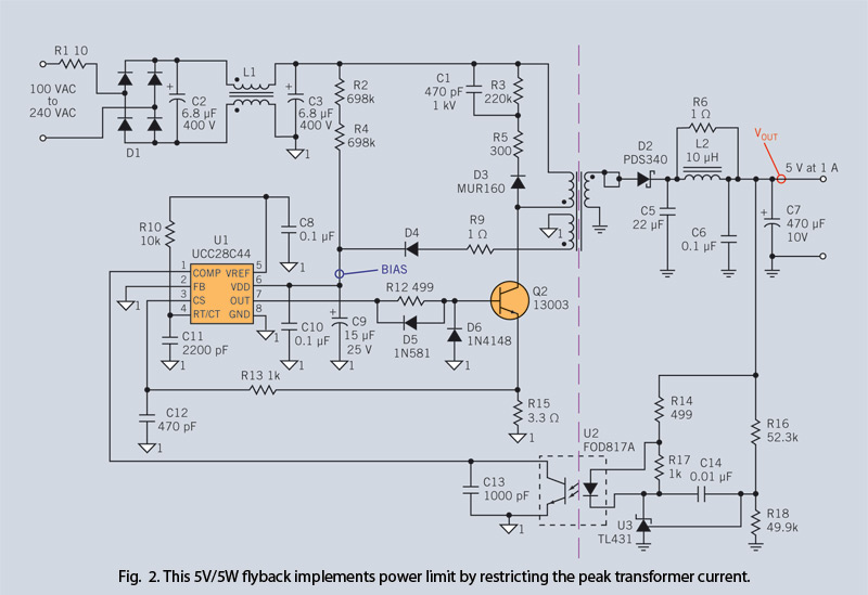
Through simple circuit modifications, designers can use peak current limiting to produce a constant current source. A constant current source is an essential component in various electronic applications, providing a steady output current regardless of load fluctuations or variations in...
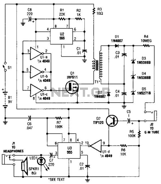
The circuit is constructed using a 4049 hex inverter (U1), two 555 oscillator/timers (U2 and U3), two transistors, a Geiger-Muller tube, and several additional support components. The first 555 timer (U2) is set up for astable operation. The output...

The circuit utilizes a transistor (VT) and a voltage regulator (VSL) to create a constant current source, employing three regulators to enhance the performance of the regulator circuit. The described circuit employs a transistor (VT) in conjunction with a voltage...