
Full complementary symmetry amplifier CL

The CL type amplifier circuit described is a sophisticated design that leverages the properties of both bipolar junction transistors (BJTs) and field-effect transistors (FETs) to achieve high fidelity audio amplification. The circuit's architecture is structured to minimize distortion while maximizing the common mode rejection ratio, which is crucial for maintaining signal integrity in audio applications. The use of complementary transistors ensures that both halves of the input signal are amplified symmetrically, which is vital for producing a balanced output.
The input stage's configuration, with FETs serving as constant current sources, enhances the linearity of the amplifier, allowing for a faithful reproduction of the input signal across a wide frequency range. This is particularly important in audio applications where signal fidelity is paramount. The feedback mechanism incorporated into the design further stabilizes the amplifier's operating point, ensuring consistent performance regardless of variations in input signal levels or environmental conditions.
Moreover, the differential input stage is designed to reject common mode signals, which are often noise and interference picked up from the environment. This is achieved through the balanced nature of the circuit, where any noise present on both input lines is effectively cancelled out in the output. The overall result is an amplifier that not only provides high gain but also maintains excellent sound quality with minimal distortion, making it suitable for high-end audio systems and professional sound reinforcement applications.
In conclusion, the CL type amplifier circuit exemplifies advanced engineering principles in electronics, focusing on efficiency, stability, and sound quality. Its design is a testament to the effectiveness of using complementary components in achieving superior audio amplification. CL type neither is a power amplifier output capacitance and feedback capacitance nor compensation capacitor amplifier circuit, all-electric road only by the transistor (or FET) and resistor. Circuit capable of generating feedback, phase shift elements are removed. From theory, this amplifier is capable of everything, without discrimination, the frequency of the input signal amplification. That is the input signal amplification in addition to outside, without any form of change. Figure 2-38 is a composed of a transistor, FET and resistor composed of a full complement of CL dual differential input amplifier circuit path.
Full complementary differential circuit by the transistor VTi ~ VT4 composition and constant FET VPi, VP2 were composed of the source, it constitutes the input stage of the circuit. FET constant current source because of its simple structure, without bias, temperature stability and higher dynamic resistance characteristics, closer to the ideal constant current source.
Using differential voltage amplifier stage balanced amplifier circuit, which consists of VTs ~ VTio composition, as the volume level of the differential circuit and dual differential input stage circuit can achieve a good match, so the best circuit in the input stage differential double-ended output state, It can greatly improve the common mode rejection ratio, and reduce the input stage of this two-stage distortion o while the differential circuit will produce a strong dc negative feedback, so that the DC operating point of the whole circuit is very stable at all levels, which is to get pretty the basic sound bar member. Balanced amplification principle is: When the positive half cycle of the signal when, VT6 and lower input is equivalent to a constant current source load, so VT8 voltage gain higher than the resistance load twelve o When the signal magnitude of the negative half cycle, VT8 and lower input is equivalent to a constant current source load, the voltage gain is increased so VT6 twelve orders of magnitude.
This high gain circuit loss really small, making the output power tubes to give greater impetus.
Related Circuits
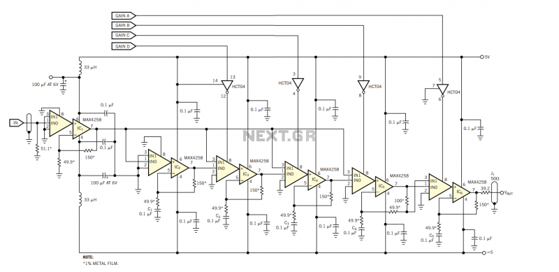
The amplifier in Figure 1 originally served as the photomultiplier preamplifier in a Doppler system intended for eventual operation in the Martian atmosphere. The design is based on a switchable array of six Maxim MAX4258 dual-channel video multiplexer-amplifiers, IC1...
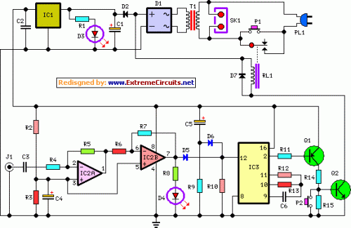
This circuit turns off an amplifier or any other device when a low-level audio signal fed to its input is absent for at least 15 minutes. Pressing P1 switches the device on, supplying power to any appliance connected to...
Often, a small amplifier is required to accommodate the needs of compact spaces. This amplifier can be configured as either mono or stereo, and its circuitry is capable of efficiently driving two small speakers. Constructing the amplifier necessitates only...
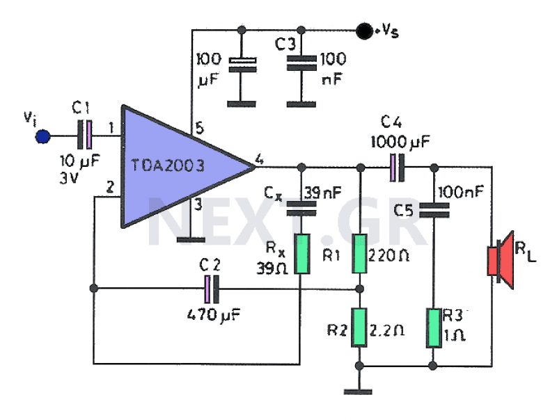
This is a handy, easy to build general purpose 50 watt amp. The amp has an input for a radio, TV, stereo or other line level device. More: It also has a phono input for a record player, guitar,...
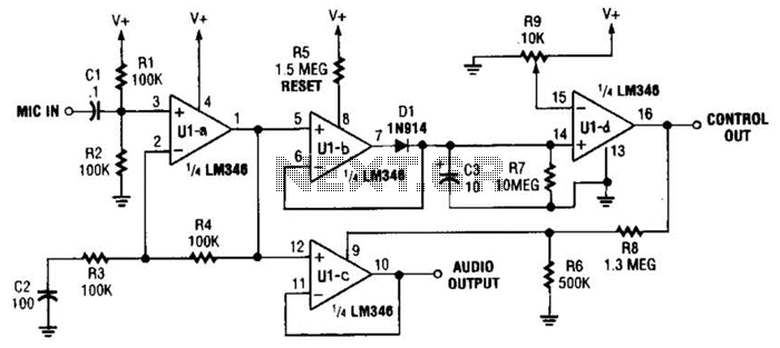
In specific applications, such as transmitters or other communications and control systems, this circuit is designed to be beneficial. It provides both audio output and DC control outputs. Additionally, R9 establishes the control threshold. The circuit in question is versatile...

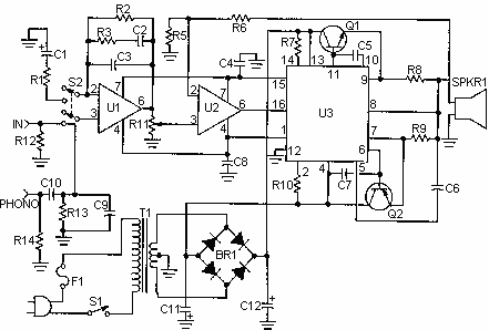
A small amplifier IC circuit has been compiled. This circuit is part of an older series and is categorized as a simple OTL (Output Transformer-Less) circuit. The presented small amplifier IC circuit is designed for applications where compact size and...