
Phase Shift Oscillator

The phase shift oscillator circuit is an essential configuration in electronic signal generation, particularly valued for its simplicity and versatility. The heart of the circuit is the common source FET amplifier, which provides the necessary gain and is characterized by its self-biasing capability. The inclusion of a bypass capacitor across the source resistor (Rs) enhances the amplifier's performance by allowing AC signals to pass while stabilizing the DC operating point.
The three-section R-C network plays a critical role in determining the oscillator's frequency and phase characteristics. Each section contributes to the overall phase shift, and the precise values of resistors and capacitors must be selected to achieve the desired oscillation frequency. The phase shift introduced by the R-C network is frequency-dependent, allowing for fine-tuning of the oscillator's output frequency.
To maintain stable oscillation, the amplifier gain must be carefully controlled. A gain of 29 ensures that the feedback loop meets the Barkhausen criteria, allowing the circuit to sustain oscillations without distortion. If the gain is excessively high, waveform distortion may occur, while a gain slightly above 29 yields a clean sinusoidal output, which is often desirable in various applications.
The circuit's design allows for easy frequency adjustments, making it suitable for a range of applications, from audio signal generation to low-frequency oscillators. By using variable capacitors and different resistor configurations, the oscillator can be tuned across multiple frequency bands, offering flexibility in signal generation tasks. The simplicity of the phase shift oscillator compared to more complex designs, such as the Wien bridge oscillator, makes it an attractive choice for engineers and hobbyists alike, facilitating efficient signal generation with minimal component requirements.We select the so called phase shift oscillator as a first example as it exemplifies verysimply the principles set forth in the previous blog post. The circuit is drawn to show clearly the amplifier and feedback network. The circuit consists of a common source FET amplifier followed by a three section R-C phase shift network.
The amplifier stage i s self-biased with a capacitor bypassed source resistor Rs and a drain bias resistance RD. The output of the last section is supplied back to the gate. If the loading of the phase-shift network on the amplifier can be assumed to be negligible, a phase shift of 180 ° between the amplified output voltage Vout and the input voltage Vin at the gate is produced by the amplifier itself. The three-section R-C phase shift network produces an additional phase shift, which is a function of frequency and equals 180 ° at some frequency of operation.
At this frequency the total phase shift from the gate around the circuit and back to gate will be exactly zero. This particular frequency will be the one at which the circuit will oscillate provided that the magnitude of the amplification is sufficiently large.
In a FET phase-shift oscillator voltage series feedback [that is, feedback voltage proportional to the output voltage Vout and supplied in series with the input signal at the gate is used. The frequency of the oscillator output depends upon the values of capacitors C and re sistors R used in the phase shift network.
Using basic RC circuit analysis technique, it can be shown that the network phase shift is 180 ° when The frequency can be adjusted over a wide range if variable capacitors are used. As well as phase shifting, the R-C network attenuates the amplifier output. Network analysisshows that when the necessary phase shift of 180 ° is obtained, this network attenuates theoutput voltage by a factor of 1/29.
This means that the amplifier must have a voltage gain of 29 or more. When the amplifier voltage gain is 29 and feedback factor of R-C network, ²= 1/29 thenthe loop gain is ² A = 1, the amplifier phase shift of 180 ° combined with the network phase shift of + 180 ° gives a loop phase shift of zero. Both of these conditions are necessary to satisfy the Barkhausen criteria. If the amplifier gain is much greater than 29, the oscillator output waveform is likely to be distorted.
When the gain is slightly greater than 29, the output is usually a reasonably pure sinusoidal. The phase shift oscillator circuit is much simpler than the Wien bridge oscillator circuit because it does not need negative feedback and the stabilization arrangements. FET phase-shift oscillator is used for generating signals over a wide frequency range. The frequency may be varied from a few Hz to 200 Hz by employing one set of re sistors with three capacitors ganged together to vary over a capacitance range in the 1 : 10 ratio.
Similarly the frequency ranges of 200 Hz to 2 kHz, 2 kHz to 20 kHz and 20 kHz to 200 kHz can be obtained by using other sets of resistors. 🔗 External reference
Related Circuits
The standard assumption is that the phase shift sections operate independently. According to the equation provided, the loop phase shift reaches -180 degrees when the phase shift of each section is 60 degrees. This condition is met when ω...
The diagram illustrates a 50 MHz oscillator functioning at its third harmonic. The collector load resistor R1 has been increased due to the rise in the quartz crystal's internal series resistance Rs, which escalates with frequency in the VHF...
To demonstrate Rincon's capability to simulate autonomous circuits, a one-transistor oscillator utilizing a phase-inverting resonance T-shape LC circuit is considered. The schematic of this simulator is illustrated in Figure 1. The design of the simulator is detailed in reference...
In this version of the oscillator, Rb is a small incandescent lamp. Typically, R1 = R2 = R and C1 = C2 = C. During normal operation, Rb self-heats to the point where its resistance is Rf/2. A Wien...
The world is full of xtal oscillators twiddled by digital designers lacking in the analog design knowledge necessary. Just look at all the PC real time clocks that lags or leads by several minutes per day. And they eat...
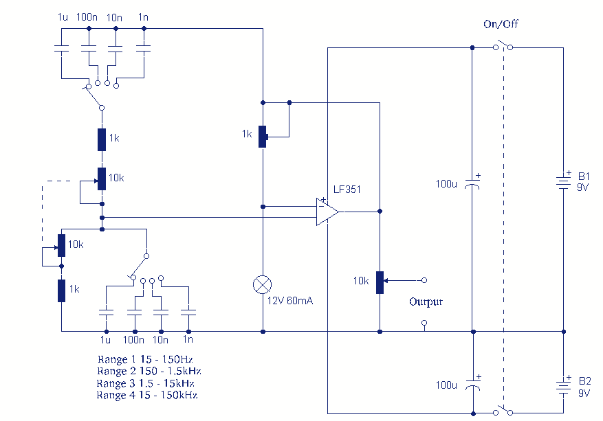
In this circuit the gain is provided by a FET type op-amp. I have used an LF351, which may be hard to obtain, but the TL071CN or TL081CN may be used and have a faster slewing rate than the...