
pll circuit

The proposed electronic schematic outlines a modernized system intended to supersede the previous BCD design, addressing its limitations while enhancing performance. The design integrates three Phase-Locked Loop (PLL) circuits, which are critical for achieving stable frequency outputs across a wide range of frequencies, up to 47 GHz. PLL circuits are known for their ability to lock onto a reference frequency and maintain a precise output frequency, making them ideal for high-frequency applications.
The architecture of the new system allows for flexible divisor factor selection, accommodating various crystal oscillator frequencies. This adaptability is particularly advantageous in applications where specific frequency outputs are required. For instance, the design can efficiently handle a crystal frequency of 94.666667 MHz, showcasing its versatility.
The elimination of the shortcomings associated with the original BCD divider chips is a focal point of this design. The previous chips often suffered from issues such as noise, drift, and limited frequency range, which could compromise overall system performance. By utilizing advanced PLL circuits, the new design aims to provide a more robust solution with improved signal integrity and reduced phase noise.
In summary, the updated system represents a significant advancement in frequency division technology, enhancing both performance and flexibility for applications in the UHF and microwave frequency ranges. The implementation of three PLL circuits, coupled with the ability to select appropriate divisor factors, positions this design as a superior alternative to its predecessors.This page will be updated as Material becomes available. This New System will essentially replace the original BCD Design originally designed by WB6IGP and N6IZW and appeared in ARRL UHF/Microwave Project Manual. Their efforts were later revised by WA6CGR. This New Design eliminates the many short Falls of the BCD Divider Chips and Implements actu ally 3 PLL Circuits that are extremely clean up to and including 47Ghz. One Huge advantage of this System is the ability to select any divisor factor appropriate for any XTAL Freq. i. e. 94. 666667Mhz to sight one example only. 🔗 External reference
Related Circuits
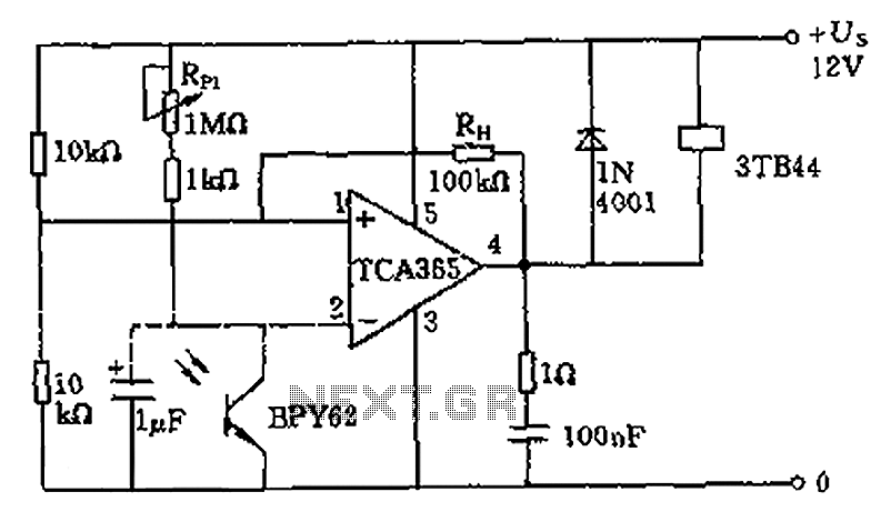
A bridge input circuit utilizing a phototransistor BPY62 and a power operational amplifier is capable of controlling power loads up to 8.5 kW. It features a voltage divider composed of two 10 kΩ resistors, creating a midpoint connection. The...
A diode, such as the IN4148, has a typical temperature coefficient of -2 mV/°C at a 1 mA diode current. Transistors Q1 and Q2 form a constant current source. Diode D1 serves as the temperature sensor. Integrated circuits ICl-a...
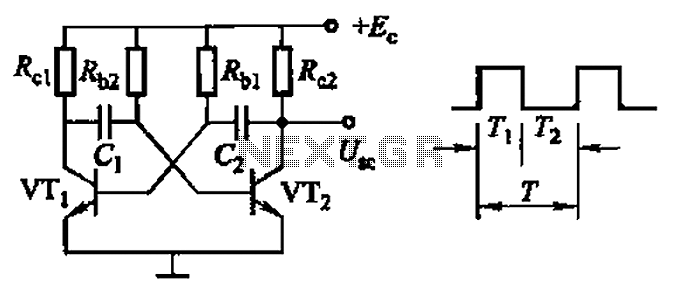
Common non-sinusoidal oscillator circuit, waveform and frequency formula - square wave oscillator - self-excited multivibrator The common non-sinusoidal oscillator circuit, specifically the square wave oscillator, is a fundamental electronic circuit utilized to generate square wave signals. It operates based on...
This gated 1-kHz oscillator provides press-to-turn-off functionality, along with waveforms available at the output of pin 3 and across capacitor C1. The gated 1-kHz oscillator circuit is designed to generate a square wave output at a frequency of 1 kHz....
As the position of the sun changes, the illumination level on the light-dependent resistors (LDRs) also varies, causing the input voltage for the window comparator to deviate from half of the supply voltage. Consequently, the output of the comparator...
The circuit depicted in Figure 3-193 illustrates a separately excited DC motor. The brake circuit is not activated; therefore, positive reversals occur alternately using a delay action relay, ensuring that the motor reverses direction after coming to a stop. The...