
Positive voltage to negative voltage converter

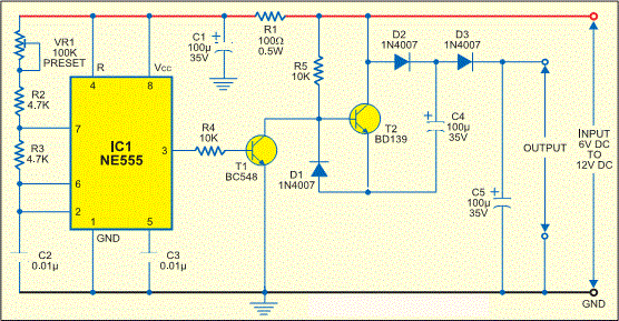
The circuit functions by utilizing the NE555 timer IC in an astable mode, generating a continuous square wave output. The frequency of oscillation is determined by the resistors and capacitors connected to the NE555, allowing for precise control over the timing characteristics. The output at pin 3 alternates between high and low states, creating a square wave signal.
During the high state of the output, capacitor C3 is charged through diode D2, which allows current to flow in one direction, ensuring that C3 accumulates charge. When the output transitions to the low state, C3 begins to discharge through D2, which simultaneously allows capacitor C4 to charge. As C4 charges, it creates a negative voltage at its cathode relative to ground, which is essential for applications requiring a dual power supply.
The diodes D1 and D2 play a crucial role in directing the flow of current and ensuring that the capacitors charge and discharge at the appropriate times. Diode D1 is responsible for isolating the negative voltage generated from the rest of the circuit, while D2 ensures that the charging and discharging processes occur without backflow, maintaining the integrity of the voltage levels.
This configuration is particularly useful in applications where a dual supply is needed, such as operational amplifiers or analog signal processing circuits, where both positive and negative voltages are required for proper operation. The NE555 timer's reliability and ease of use make this circuit a popular choice for generating negative voltages in various electronic applications.This circuit diagram shows how to obtain a negative voltage from a positive voltage supply. Another advantage of this circuit is that, the negative voltage together with the original positive supply can be used to simulate a dual supply. The circuit is based on timer IC NE555. The NE555 is wired as an astable multivibrator operating at around 1 KH z. The square wave output if available at pin no 3 of the IC. During the positive half of the square wave, capacitor C3 charges through diode D2. When the output of IC is at zero the C3 discharges through diode D2 and the capacitor C4 gets charged. As a result of this the voltage at the junction of the anode of D1 and cathode of C4 will be always negative with respect to the ground.
🔗 External reference
Related Circuits
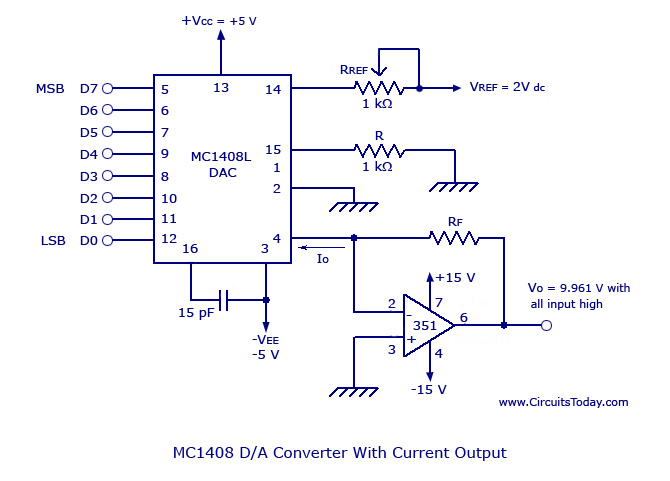
Monolithic/Hybrid Digital to Analog Converters using MC 1408 IC, SE/NE 5018, Specifications and Applications. Monolithic and hybrid digital-to-analog converters (DACs) are integral components in various electronic systems, facilitating the conversion of digital signals into corresponding analog voltages or currents. The...
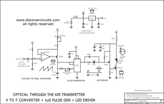
This circuit receives the signal from the amplifier and emits powerful 1μs infrared light pulses from a low-cost LED, which are frequency modulated by the audio information. The 10kHz center frequency of the pulse stream is sufficiently low, allowing...
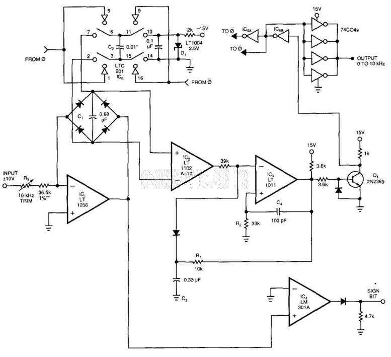
This voltage-to-frequency converter (VFC) accepts bipolar AC inputs. For -10 to +10 V inputs, the converter produces a proportional 0 to 10 kHz output. Linearity is 0.04%, and the temperature coefficient (TC) is approximately 50 ppm/°C. To understand the...
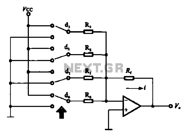
An A/D converter circuit can be represented by a simplified schematic, which illustrates a parallel type A/D converter. The term "median" refers to the number of bits in the digital signal output. The figure displays four A/D converters utilizing...

Logic overvoltage protection power supply. Refer to the designated page for an explanation of the power supply circuit diagram mentioned above. The logic overvoltage protection power supply is designed to safeguard sensitive electronic components from voltage spikes that could potentially...
All miniature electronic devices operate on batteries. Some require higher than standard battery voltages for efficient operation. When a battery of the required voltage is unavailable, additional cells must be connected in series to increase the DC voltage, which...