
Power Supply

This is why the zener diode in the diagram is rated at 15 V. Many regulators produced by National Semiconductor have an integral on/off switch, and this is used in the present circuit. The input is intended for TTL signals, and usually consists of a transistor whose base is accessible externally.
This means that a higher switching voltage may be applied via a series resistor: the value of this in the present circuit is 22 k. When the voltage across the capacitor reaches a level of about 17 V, transistor T1 comes on, whereupon the regulator is enabled.
linear power supply, shown in the schematic, provides 0-30 volts, at one amp, maximum, using a discrete transistor regulator with op amp feedback to control the output voltage. The supply was constructed in 1975-6 & has a constant current mode that is used to recharge batteries.
With reference to the schematic, lamp, LP2, is a power on indicator. The other lamp (lower) lights when the unit reaches its preset current limit. R5, C2, & Q10 (TO-3 case) operate as a capacitor multiplier. The 36 volt zen-er across C2 limits the maximum supply voltage to the op amps supply pins. D5, C4, C5, R15, & R16 provide a tiny amount of negative supply for the op amps so that the op amps can operate down to zero volts at the output pins (pins 6). A more modern design might eliminate these four parts & use a CMOS rail-to-rail op-amp. Current limit is set by R3, D1, R4, R6, Q12, R10, & R13 providing a bias to U2 that partially turns off transistors Q9 & Q11 when the current limit is reached.
R4 is a front panel potentiometer that sets the current limit, R22 is a front panel potentiometer that sets the output voltage (0-30 volts), & R11 is an internal trim-pot for calibration. The meter is a one milliamp meter with an internal resistance of 40 ohms. Switch S1 determines whether the meter reads 0-30 volts, or 0-1 amp. A more new circuit might use a single IC regulator, such as the MC78XX, or MC79XX series, immediately after the half wave rectifier, to replace about 30 parts, or at least a high precision zen-er diode to replace D10 as the voltage reference.
The LM4040 is such voltage reference & has excellent stability over temperature. IC regulators such as the MC78XX series may finally become obsolete as newer IC regulators are designed, however, discrete transistors, op-amps, & zeners are more generic, have an extended production lifespan, & permit the designer to demonstrate that they understands the principles of linear regulated power supply operation. One of the basic building blocks of electronics project is building your own DC power supplies from an AC source of 110 V.
A. C or 220 V. A. C. The common DC voltages that are necessary to power up the devices are usually in the range of three V DC to 30 V DC. Usually the fixed types of DC voltages are 5V, 9V, 12V, 15V & 18V DC. With the advancement of know-how, lots of devices are using one. 8 V DC these days. S M P S is becoming common these days as the demand for miniaturization due to space constraints increases.
Take note that for linear power supply projects, you need to make use of a step down power transformer to step down the AC voltage from the line voltage of 110 V. A. C or 220 V. A. C before using it to supply to the diode bridge. In recent years, the use of switch mode power supply (SMPS) has become more comon as more applications demand for greater power eficiency.
It makes use of semiconductor (mostly MOSFET) fast switches to switch DC input that has been rectified at high frequency. The advantages of high frequency switching are that it reduces the size of inductor, capacitors & transformer used.
Other advantages of switching power supply over linear power supply are : The setback of using SMPS compared to linear power supply is that it generates electrical noise which contributes to electromagnetic compatibility design issues & more part count. The SMPS circuit below from Power Integration makes use of LNK304 as its high frequency switch. Take note that this circuit is non isolated type which means that the output is not electrically isolated from the input & all testing ought to be completed using an isolation transformer to provide the AC line input to the board.
Many times the hobbyist desires to have a simple, dual power supply for a project. Existing power supplies may be large either in power output or physical size. a simple Dual Power Supply is necessary. For most non-critical applications the best & simplest choice for a voltage regulator is the 3-terminal type. The three terminals are input, ground & output. The 78xx & 79xx series can provide up to 1A load current & it have on chip circuitry to prevent damage in the event of over heating or excessive current.
That is, the chip basically shuts down than blowing out. These regulators are cheap, simple to make use of, & they make it practical to design a method with plenty of P C Bs in which an unregulated supply is brought in & regulation is done locally on each circuit board. This Dual Power Supply project provides a dual power supply. With the appropriate choice of transformer & 3-terminal voltage regulator pairs you can basically build a tiny power supply delivering up to amp at +/- 5V, +/- 9V, +/- 12V, +/-15V or +/-18V.
You require to provide the middle tapped transformer and the 3-terminal pair of regulators you require:7805 & 7905, 7809 & 7909, 7812 & 7912, 7815 & 7915or 7818 & 7918. Note that the + & regulators do not must be matched: you can for example, use a +5v & -9V pair. However, the positive regulator must be a 78xx regulator, & the negative a 79xx. They have built in plenty of safety in to this project so it ought to give plenty of years of continuous service.
This Dual Power Supply design makes use of a full wave bridge rectifier coupled with a centre-tapped transformer. A transformer with a power output rated at at least 7VA ougwo watts. A simple calculation 🔗 External reference
Related Circuits
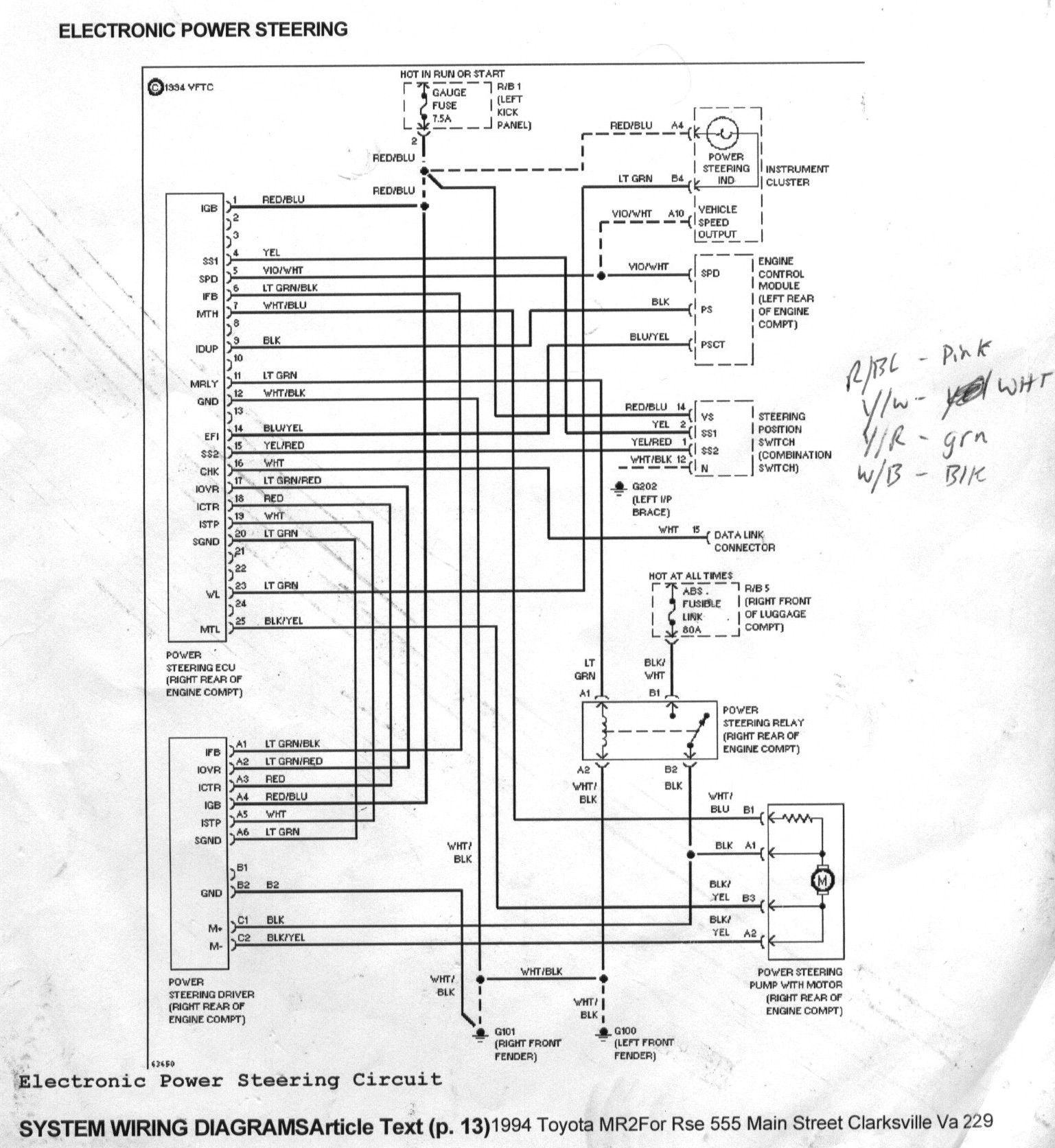
The goal was to control the MR2 power steering pump to reduce noise and power consumption, as it operates at full throttle continuously. Designing a custom motor controller was not feasible due to a lack of expertise, and off-the-shelf...
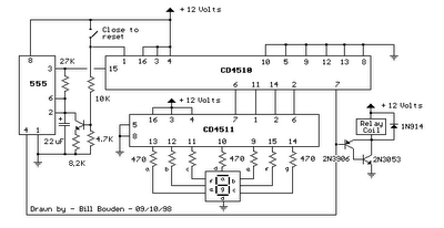
When the switch is opened, the timer generates an approximate 1-second clock signal, decrementing the counter until it reaches a count of zero. Upon reaching zero, the carry-out signal at pin 7 of the counter goes low, energizing a...
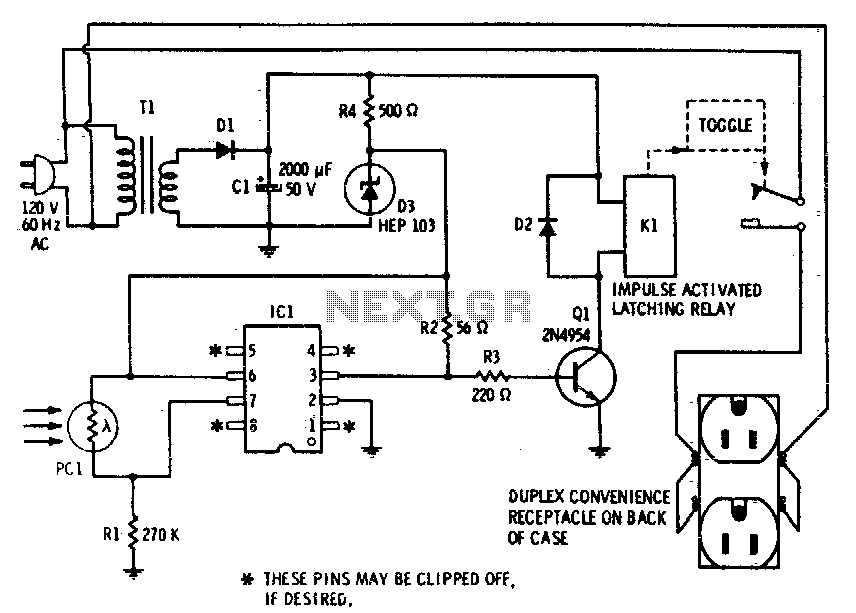
This device enables remote control of AC-powered appliances by utilizing the beam of a flashlight as a triggering mechanism. A key feature of this gadget is its memory function; activating it once supplies power to the device, and it...
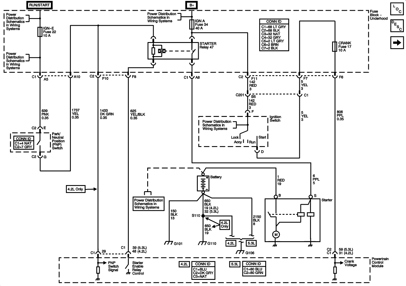
When the weather is hot and the sun is shining, the car fails to start, and the radio, keyless entry, power windows, power locks, and power seats do not function. However, after sunset, everything operates normally. It is important...
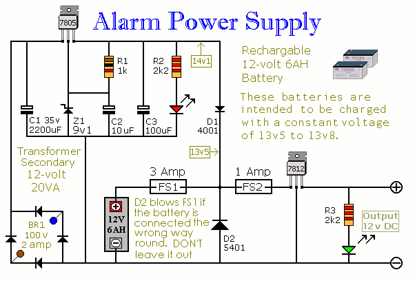
This power supply is designed for the Modular Burglar Alarm but is suitable for various applications. It delivers a 12-volt output with a maximum current of 1 amp. In case of a mains failure, the backup battery activates immediately,...
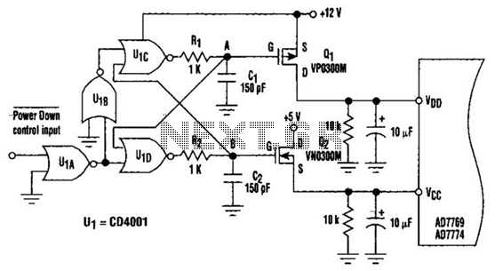
This circuit adds a power-down function to analog I/O ports, such as the AD7769 and AD7774. Additionally, the diodes typically required to protect the devices against power-supply mis-sequencing can be eliminated. In this design, MOSFETs Q1 and Q2 switch...