
Simple Power Down Circuit Circuit

Specifically, raising the power-down control causes the output of U1C to go low, resulting in capacitor C1 discharging exponentially with a time constant. As the voltage on C1 decreases, two key events occur. First, this creates a negative gate-source voltage on the P-channel MOSFET Q1, turning it on. Second, this action drives the output of U1D high. With U1D's output high, capacitor C2 charges exponentially to approximately 12 V, applying a positive gate-source voltage that turns on Q2. In the power-down mode, when the power-down control is set low, the RC circuits and their associated delays operate in reverse. Consequently, capacitor C2 discharges to the logic input of U1C before C1 can charge, resulting in Q2 turning off before Q1.
This circuit is designed to effectively manage the power sequencing of analog I/O devices, ensuring that they remain protected from potential damage caused by improper power application. The use of MOSFETs for switching provides a low-resistance path when activated, minimizing power loss and improving efficiency. The cross-coupled NOR gates serve a critical role in controlling the timing of the power application and removal, thereby ensuring that the sequence is maintained within safe operational limits.
The power-down control mechanism is crucial for systems where power management is essential. By integrating this function, the circuit not only enhances the reliability of the connected devices but also simplifies the overall design by eliminating the need for additional protective diodes. The careful design of the RC timing networks ensures that the transition between power states is smooth, thus protecting sensitive components from voltage spikes and ensuring stable operation during power cycling. This circuit, adds a power-down function to analog I/O ports (for example, the AD7769 and AD7774). Moreover, the diodes ordinarily needed to protect the devices against power-supply mis-sequencing can be eliminated (see the figure).In the circuit, MOSFETs Ql and Q2 switch the +5- and +12-V supplies, respectively, in a sequence controlled by two cross-coupled CD4001 CMOS NOR gates (U1C and U1D). The sequence in which power is applied is important: The controlled circuits may be damaged anytime Vcc exceeds VDD + 0.3 V.
Consequently, the NOR gates must be powered from a 12-V supply throughout the power-down sequence.Bringing the power down control high (+5 V) applies power to the controlled circuit by turning on all MOSFETs. Specifically, raising the power down brings the output of U1C low, causing capacitor CI to discharge VOL exponentially with time constant0. As the voltage on CI falls, two events occur. First, it puts a negative gate-source voltage on P-channel Ql, turning it on.Second, it causcs output gate U1D to go high.
With the output of U1D high, capacitor C2 charges exponentially to VOHabout 12-Vapplying a positive gate-source voltage to turn on Q2. In the power down mode, the Power Down control is brought low and the RC circuits and their delays work in reverse.
Consequently, capacitor C2 discharges to the logic input of U1C before CI can charge. Hence, Q2 turns off before Ql.
Related Circuits
A resistor-capacitor circuit designed to prevent spark blowout. The coil's magnetic energy is converted into electrical energy stored in the capacitance C, effectively suppressing sparks and enhancing safety. The circuit is capable of functioning normally even with reverse polarity....
This is a compact and straightforward FM radio receiver capable of tuning into local FM stations. Its minimalistic design renders it suitable for various applications. The FM radio receiver circuit typically consists of several key components that work together to...
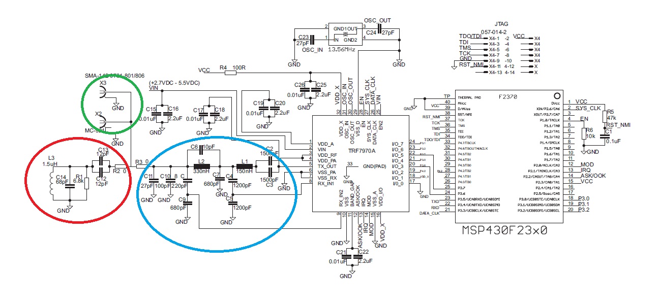
The "green area" is designated for the placement of the TRF7970A's antenna, which should be connected between two 0-ohm resistors. The antenna can be constructed step by step following the guidelines in the document "Antenna Matching for the TRF7960...
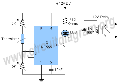
A thermistor is utilized in the circuit for heat sensing, while two 5K variable resistors are incorporated to calibrate the circuit for activating the relay at the desired temperature. The inclusion of a 1N4007 diode across the relay serves...
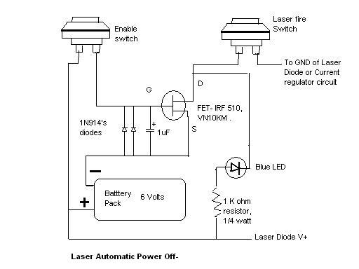
Here is the automatic laser power-off circuit schematic. This circuit features a visible power indication. In this case, the ground is connected on one side. The automatic laser power-off circuit is designed to enhance safety and efficiency in laser applications...

This 5.1 surround amplifier circuit schematic utilizes the IC AN7168 as the primary component. The circuit requires a minimum voltage of 12V and a maximum voltage of 24V, with a recommendation of 12V due to the voltage ratings of...